SNVSAF7B August 2016 – February 2017 LM27762
PRODUCTION DATA.
- 1 Features
- 2 Applications
- 3 Description
- 4 Revision History
- 5 Pin Configuration and Functions
- 6 Specifications
- 7 Detailed Description
-
8 Application and Implementation
- 8.1 Application Information
- 8.2
Typical Application
- 8.2.1 Design Requirements
- 8.2.2 Detailed Design Procedure
- 8.2.3 Application Curves
- 9 Power Supply Recommendations
- 10Layout
- 11Device and Documentation Support
- 12Mechanical, Packaging, and Orderable Information
1 Features
- Generates Low-Noise Adjustable Positive Supply Voltage Between 1.5 V and 5 V and Negative Supply Voltage Between –1.5 V and –5 V
- Input Voltage Range 2.7 V to 5.5 V
- ±250-mA Output Current
- Inverting Charge Pump Followed by Negative LDO
- 2-MHz Low-Noise Fixed-Frequency Operation
- 2.5-Ω Inverter Output Impedance, VIN = 5 V
- Negative LDO Dropout Voltage 30 mV at 100 mA, VOUT = –5 V
- Positive LDO with 45-mV Dropout Voltage at 100 mA, VOUT = 5 V
- 390-µA Quiescent Current (Typical)
- Shutdown Quiescent Current to 0.5 µA (Typical)
- Current Limit and Thermal Protection
- Power Good Pin (Active Low)
- Create a Custom Design Using the LM27762 With the WEBENCH® Power Designer
2 Applications
- Hi-Fi Audio Headphone Amplifiers
- Operational Amplifier Power Biasing
- Powering Data Converters
- Wireless Communication Systems
- Interface Power Supplies
- Handheld Instrumentation
3 Description
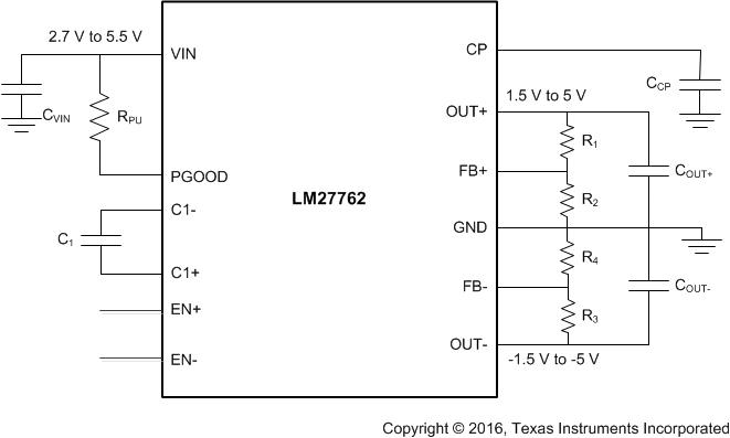
The LM27762 delivers very low-noise positive and negative outputs that are adjustable between ±1.5 V and ±5 V. Input-voltage range is from 2.7 V to 5.5 V, and output current goes up to ±250 mA. With an operating current of only 390 µA and 0.5-µA typical shutdown current, the LM27762 provides ideal performance for power amplifier and DAC bias and other high-current, low-noise negative voltage needs. The device provides a small solution size with few external components.
Negative voltage is generated by a regulated inverting charge pump followed by a low-noise negative LDO. The inverting charge pump of the LM27762 device operates at 2-MHz (typical) switching frequency to reduce output resistance and voltage ripple. Positive voltage is generated from the input by a low-noise positive LDO.
Positive and negative outputs of LM27762 have dedicated enable inputs. These outputs support independent timing for the positive and negative rails for specific system power-sequence needs. Enable inputs can be also shorted together and connected to the input voltage. The LM27762 has an optional Power Good feature.
Device Information(1)
| PART NUMBER | PACKAGE | BODY SIZE (NOM) |
|---|---|---|
| LM27762 | WSON (12) | 2.00 mm × 3.00 mm |
- For all available packages, see the orderable addendum at the end of the data sheet.
space
Simplified Schematic
