SNVSAB5A September   2017  – June 2021 LP87332A-Q1

PRODUCTION DATA  

  1. Features
  2. Applications
  3. Description
  4. Revision History
  5. Pin Configuration and Functions
  6. Specifications
    1. 6.1 Absolute Maximum Ratings
    2. 6.2 ESD Ratings
    3. 6.3 Recommended Operating Conditions
    4. 6.4 Thermal Information
    5. 6.5 Electrical Characteristics
    6. 6.6 I2C Serial Bus Timing Parameters
    7. 6.7 Typical Characteristics
  7. Detailed Description
    1. 7.1 Overview
    2. 7.2 Functional Block Diagram
    3. 7.3 Feature Description
      1. 7.3.1  DC/DC Converters
        1. 7.3.1.1 Overview
        2. 7.3.1.2 Transition Between PWM and PFM Modes
        3. 7.3.1.3 Buck Converter Load Current Measurement
        4. 7.3.1.4 Spread-Spectrum Mode
      2. 7.3.2  Sync Clock Functionality
      3. 7.3.3  Low-Dropout Linear Regulators (LDOs)
      4. 7.3.4  Power-Up
      5. 7.3.5  Regulator Control
        1. 7.3.5.1 Enabling and Disabling Regulators
        2. 7.3.5.2 Changing Output Voltage
      6. 7.3.6  Enable and Disable Sequences
      7. 7.3.7  Device Reset Scenarios
      8. 7.3.8  Diagnosis and Protection Features
        1. 7.3.8.1 Power-Good Information (PGOOD pin)
          1. 7.3.8.1.1 PGOOD Pin Gated Mode
          2. 7.3.8.1.2 PGOOD Pin Continuous Mode
          3. 7.3.8.1.3 PGOOD Pin Inactive Mode
        2. 7.3.8.2 Warnings for Diagnosis (Interrupt)
          1. 7.3.8.2.1 Output Power Limit
          2. 7.3.8.2.2 Thermal Warning
        3. 7.3.8.3 Protection (Regulator Disable)
          1. 7.3.8.3.1 Short-Circuit and Overload Protection
          2. 7.3.8.3.2 Overvoltage Protection
          3. 7.3.8.3.3 Thermal Shutdown
        4. 7.3.8.4 Fault (Power Down)
          1. 7.3.8.4.1 Undervoltage Lockout
      9. 7.3.9  Operation of the GPO Signals
      10. 7.3.10 Digital Signal Filtering
    4. 7.4 Device Functional Modes
      1. 7.4.1 Modes of Operation
    5. 7.5 Programming
      1. 7.5.1 I2C-Compatible Interface
        1. 7.5.1.1 Data Validity
        2. 7.5.1.2 Start and Stop Conditions
        3. 7.5.1.3 Transferring Data
        4. 7.5.1.4 I2C-Compatible Chip Address
        5. 7.5.1.5 Auto-Increment Feature
    6. 7.6 Register Maps
      1. 7.6.1 Register Descriptions
        1. 7.6.1.1  DEV_REV
        2. 7.6.1.2  OTP_REV
        3. 7.6.1.3  BUCK0_CTRL_1
        4. 7.6.1.4  BUCK0_CTRL_2
        5. 7.6.1.5  BUCK1_CTRL_1
        6. 7.6.1.6  BUCK1_CTRL_2
        7. 7.6.1.7  BUCK0_VOUT
        8. 7.6.1.8  BUCK1_VOUT
        9. 7.6.1.9  LDO0_CTRL
        10. 7.6.1.10 LDO1_CTRL
        11. 7.6.1.11 LDO0_VOUT
        12. 7.6.1.12 LDO1_VOUT
        13. 7.6.1.13 BUCK0_DELAY
        14. 7.6.1.14 BUCK1_DELAY
        15. 7.6.1.15 LDO0_DELAY
        16. 7.6.1.16 LDO1_DELAY
        17. 7.6.1.17 GPO_DELAY
        18. 7.6.1.18 GPO2_DELAY
        19. 7.6.1.19 GPO_CTRL
        20. 7.6.1.20 CONFIG
        21. 7.6.1.21 PLL_CTRL
        22. 7.6.1.22 PGOOD_CTRL_1
        23. 7.6.1.23 PGOOD_CTRL_2
        24. 7.6.1.24 PG_FAULT
        25. 7.6.1.25 RESET
        26. 7.6.1.26 INT_TOP_1
        27. 7.6.1.27 INT_TOP_2
        28. 7.6.1.28 INT_BUCK
        29. 7.6.1.29 INT_LDO
        30. 7.6.1.30 TOP_STAT
        31. 7.6.1.31 BUCK_STAT
        32. 7.6.1.32 LDO_STAT
        33. 7.6.1.33 TOP_MASK_1
        34. 7.6.1.34 TOP_MASK_2
        35. 7.6.1.35 BUCK_MASK
        36. 7.6.1.36 LDO_MASK
        37. 7.6.1.37 SEL_I_LOAD
        38. 7.6.1.38 I_LOAD_2
        39. 7.6.1.39 I_LOAD_1
  8. Application and Implementation
    1. 8.1 Application Information
    2. 8.2 Typical Application
      1. 8.2.1 Design Requirements
        1. 8.2.1.1 Inductor Selection
        2. 8.2.1.2 Buck Input Capacitor Selection
        3. 8.2.1.3 Buck Output Capacitor Selection
        4. 8.2.1.4 LDO Input Capacitor Selection
        5. 8.2.1.5 LDO Output Capacitor Selection
      2. 8.2.2 Detailed Design Procedure
      3. 8.2.3 Application Curves
  9. Power Supply Recommendations
  10. 10Layout
    1. 10.1 Layout Guidelines
    2. 10.2 Layout Example
  11. 11Device and Documentation Support
    1. 11.1 Device Support
      1. 11.1.1 Third-Party Products Disclaimer
    2. 11.2 Receiving Notification of Documentation Updates
    3. 11.3 Support Resources
    4. 11.4 Trademarks
    5. 11.5 Electrostatic Discharge Caution
    6. 11.6 Glossary
  12. 12Mechanical, Packaging, and Orderable Information

Features

  • AEC-Q100 qualified with the following results:
    • Device temperature grade 1: –40°C to +125°C ambient operating temperature
  • Input voltage: 2.8 V to 5.5 V
  • Two high-efficiency step-down DC/DC converters:
    • Output voltage: 0.7 V to 3.36 V
    • Maximum output current 3 A
    • Programmable output-voltage slew rate from 0.5 mV/µs to 10 mV/µs
    • 2-MHz switching frequency
    • Spread-spectrum mode and phase interleaving for EMI reduction
  • Two linear regulators:
    • Input voltage: 2.5 V to 5.5 V
    • Output voltage: 0.8 V to 3.3 V
    • Maximum output current 300 mA
  • Configurable general-purpose output signals (GPO, GPO2)
  • Interrupt function with programmable masking
  • Programmable power-good signal (PGOOD)
  • Output short-circuit and overload protection
  • Overtemperature warning and protection
  • Overvoltage protection (OVP) and undervoltage lockout (UVLO)
  • 28-pin, 5-mm × 5-mm VQFN package with wettable flanks
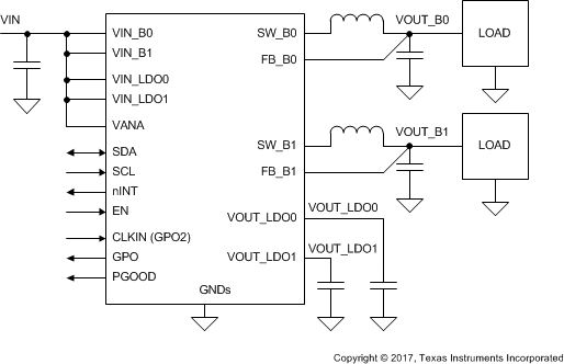
GUID-08BB30EC-A301-4C85-B8AC-94B974860794-low.gif Simplified Schematic