SNLS416D June 2012 – January 2015 DS90UB927Q-Q1
PRODUCTION DATA.
- 1 Features
- 2 Applications
- 3 Description
- 4 Revision History
- 5 Pin Configuration and Functions
-
6 Specifications
- 6.1 Absolute Maximum Ratings
- 6.2 ESD Ratings
- 6.3 Recommended Operating Conditions
- 6.4 Thermal Information
- 6.5 DC Electrical Characteristics
- 6.6 AC Electrical Characteristics
- 6.7 Electrical Characteristics: DC and AC Serial Control Bus
- 6.8 Timing Requirements for the Serial Control Bus
- 6.9 Timing Requirements - DC and AC Serial Control Bus Characteristics
- 6.10 Typical Characteristics
-
7 Detailed Description
- 7.1 Overview
- 7.2 Functional Block Diagram
- 7.3
Feature Description
- 7.3.1 High-Speed Forward Channel Data Transfer
- 7.3.2 Low-Speed Back Channel Data Transfer
- 7.3.3 Common Mode Filter Pin (CMF)
- 7.3.4 Video Control Signals
- 7.3.5 EMI Reduction Features
- 7.3.6 Built-In Self Test (BIST)
- 7.3.7 Forward Channel and Back Channel Error Checking
- 7.3.8 Internal Pattern Generation
- 7.3.9 Remote Auto Power-Down Mode
- 7.3.10 Input RxCLKIN Loss Detect
- 7.3.11 Serial Link Fault Detect
- 7.3.12 Interrupt Pin (INTB)
- 7.3.13 General-Purpose I/O
- 7.3.14 I2S Audio Interface
- 7.3.15 Additional Features
- 7.4 Device Functional Modes
- 7.5 Programming
- 7.6 Register Maps
- 8 Application and Implementation
- 9 Power Supply Recommendations
- 10Layout
- 11Device and Documentation Support
- 12Mechanical, Packaging, and Orderable Information
1 Features
- Bidirectional Control Channel Interface with I2C-compatible Serial Control Bus
- Low EMI FPD-Link Video Input
- Supports High Definition (720p) Digital Video Format
- 5-MHz to 85-MHz PCLK Supported
- RGB888 + VS, HS, DE and I2S Audio Supported
- Up to 4 I2S Digital Audio Inputs for Surround Sound Applications
- 4 Bidirectional GPIO Channels with 2 Dedicated Pins
- Single 3.3-V Supply with 1.8-V or 3.3-V Compatible LVCMOS I/O Interface
- AC-Coupled STP Interconnect Up to 10 Meters
- DC-Balanced and Scrambled Data With Embedded Clock
- Supports Repeater Application
- Internal Pattern Generation
- Low Power Modes Minimize Power Dissipation
- Automotive Grade Product: AEC-Q100 Grade 2 Qualified
- >8-kV HBM and ISO 10605 ESD Rating
- Backward Compatible Modes
2 Applications
- Automotive Displays for Navigation
- Rear Seat Entertainment Systems
- Automotive Driver Assistance
- Automotive Megapixel Camera Systems
3 Description
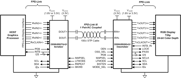
The DS90UB927Q-Q1 serializer, in conjunction with a DS90UB928Q-Q1 or DS90UB926Q-Q1 deserializer, provides a complete digital interface for concurrent transmission of high-speed video, audio, and control data for automotive display and image sensing applications.
The chipset is ideally suited for automotive video display systens with HD formats and automotive vision systems with megapixel resolutions. The DS90UB927Q-Q1 incorporates an embedded bidirectional control channel and low latency GPIO controls. This device translates a FPD-Link video interface into a single-pair high-speed serialized interface. The FPD-Link III serial bus scheme supports full duplex, high speed forward channel data transmission and low-speed back channel communication over a single differential link. Consolidation of audio, video, and control data over a single differential pair reduces the interconnect size and weight, while also eliminating skew issues and simplifying system design.
The DS90UB927Q-Q1 serializer embeds the clock and level shifts the signals to high-speed differential signaling. Up to 24 RGB data bits are serialized along with three video control signals, and up to four I2S data inputs.
The FPD-Link data interface allows for easy interfacing with data sources while also minimizing EMI and bus width. EMI on the high-speed FPD-Link III bus is minimized using low voltage differential signaling, data scrambling and randomization, and DC-balancing.
Device Information(1)
| PART NUMBER | PACKAGE | BODY SIZE (NOM) |
|---|---|---|
| DS90UB927Q-Q1 | WQFN (40) | 6.00 mm x 6.00 mm |
- For all available packages, see the orderable addendum at the end of the datasheet.
Application Diagram
