SNLS044D May 2000 – July 2016 DS90LV047A
PRODUCTION DATA.
- 1 Features
- 2 Applications
- 3 Description
- 4 Revision History
- 5 Pin Configuration and Functions
- 6 Specifications
- 7 Parameter Measurement Information
- 8 Detailed Description
- 9 Application and Implementation
- 10Power Supply Recommendations
- 11Layout
- 12Device and Documentation Support
- 13Mechanical, Packaging, and Orderable Information
1 Features
- >400-Mbps (200 MHz) Switching Rates
- Flow-Through Pinout Simplifies PCB Layout
- 300-ps Typical Differential Skew
- 400-ps Maximum Differential Skew
- 1.7-ns Maximum Propagation Delay
- 3.3-V Power Supply Design
- ±350-mV Differential Signaling
- Low Power Dissipation (13 mW at 3.3-V Static)
- Interoperable With Existing 5-V LVDS Receivers
- High impedance on LVDS Outputs on Power Down
- Conforms to TIA/EIA-644 LVDS Standard
- Industrial Operating Temperature Range
(−40°C to +85°C) - Available in Surface Mount SOIC and Low Profile TSSOP Package
2 Applications
- Multifunction Printers
- LVDS – LVCMOS Translation
3 Description
The DS90LV047A device is a quad CMOS flow-through differential line driver designed for applications requiring ultra-low power dissipation and high data rates. The device is designed to support data rates in excess of 400 Mbps (200 MHz) using Low Voltage Differential Signaling (LVDS) technology.
The DS90LV047A accepts low voltage TTL/CMOS input levels and translates them to low voltage
(350 mV) differential output signals. In addition, the driver supports a TRI-STATE function that may be used to disable the output stage, disabling the load current, and thus dropping the device to an ultra low idle power state of 13 mW typical. The DS90LV047A has a flow-through pinout for easy PCB layout.
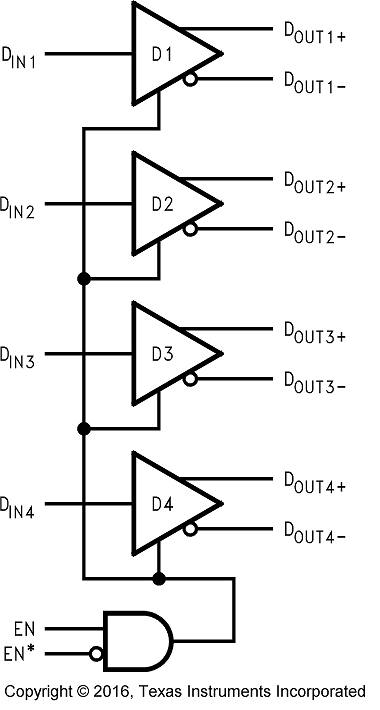
The EN and EN* inputs are ANDed together and control the TRI-STATE outputs. The enables are common to all four drivers. The DS90LV047A and companion line receiver (DS90LV048A) provide a new alternative to high power psuedo-ECL devices for high speed point-to-point interface applications.
Device Information(1)
| PART NUMBER | PACKAGE | BODY SIZE (NOM) |
|---|---|---|
| DS90LV048A | SOIC (16) | 9.90 mm × 3.91 mm |
| TSSOP (16) | 5.00 mm × 4.40 mm |
- For all available packages, see the orderable addendum at the end of the data sheet.
Functional Diagram
