SLVSBM1H June   2013  – November 2016 TPS65132 , TPS65132S

UNLESS OTHERWISE NOTED, this document contains PRODUCTION DATA.  

  1. Features
  2. Applications
  3. Description
  4. Revision History
  5. Device Comparison Table
  6. Pin Configuration and Functions
  7. Specifications
    1. 7.1 Absolute Maximum Ratings
    2. 7.2 ESD Ratings
    3. 7.3 Recommended Operating Conditions
    4. 7.4 Thermal Information
    5. 7.5 Electrical Characteristics
    6. 7.6 I2C Interface Timing Requirements / Characteristics
    7. 7.7 Typical Characteristics
  8. Detailed Description
    1. 8.1 Overview
    2. 8.2 Functional Block Diagram
    3. 8.3 Feature Description
      1. 8.3.1 Undervoltage Lockout (UVLO)
      2. 8.3.2 Active Discharge
      3. 8.3.3 Boost Converter
        1. 8.3.3.1 Boost Converter Operation
        2. 8.3.3.2 Power-Up And Soft-Start (Boost Converter)
        3. 8.3.3.3 Power-Down (Boost Converter)
        4. 8.3.3.4 Isolation (Boost Converter)
        5. 8.3.3.5 Output Voltage (Boost Converter)
        6. 8.3.3.6 Advanced Power-Save Mode For Light-Load Efficiency And PFM
      4. 8.3.4 LDO Regulator
        1. 8.3.4.1 LDO Operation
        2. 8.3.4.2 Power-Up And Soft-Start (LDO)
        3. 8.3.4.3 Power-Down And Discharge (LDO)
        4. 8.3.4.4 Isolation (LDO)
        5. 8.3.4.5 Setting The Output Voltage (LDO)
      5. 8.3.5 Negative Charge Pump
        1. 8.3.5.1 Operation
        2. 8.3.5.2 Power-Up And Soft-Start (CPN)
        3. 8.3.5.3 Power-Down And Discharge (CPN)
        4. 8.3.5.4 Isolation (CPN)
        5. 8.3.5.5 Setting The Output Voltage (CPN)
    4. 8.4 Device Functional Modes
      1. 8.4.1 Enabling and Disabling the Device
    5. 8.5 Programming
      1. 8.5.1 I2C Serial Interface Description
      2. 8.5.2 I2C Interface Protocol
    6. 8.6 Register Maps
      1. 8.6.1 Registers
        1. 8.6.1.1 VPOS Register - Address: 0x00
        2. 8.6.1.2 VNEG Register - Address 0x01
        3. 8.6.1.3 DLYx Register - Address 0x02 (Only valid for TPS65132Sx)
        4. 8.6.1.4 APPS - SEQU - SEQD - DISP - DISN Register - Address 0x03
        5. 8.6.1.5 Control Register - Address 0xFF
      2. 8.6.2 Factory Default Register Value
  9. Application and Implementation
    1. 9.1 Application Information
    2. 9.2 Typical Applications
      1. 9.2.1 Low-current Applications (≤ 40 mA)
        1. 9.2.1.1 Design Requirements
        2. 9.2.1.2 Detailed Design Procedure
          1. 9.2.1.2.1 Sequencing
          2. 9.2.1.2.2 Boost Converter Design Procedure
            1. 9.2.1.2.2.1 Inductor Selection (Boost Converter)
            2. 9.2.1.2.2.2 Input Capacitor Selection (Boost Converter)
            3. 9.2.1.2.2.3 Output Capacitor Selection (Boost Converter)
          3. 9.2.1.2.3 Input Capacitor Selection (LDO)
          4. 9.2.1.2.4 Output Capacitor Selection (LDO)
          5. 9.2.1.2.5 Input Capacitor Selection (CPN)
          6. 9.2.1.2.6 Output Capacitor Selection (CPN)
          7. 9.2.1.2.7 Flying Capacitor Selection (CPN)
        3. 9.2.1.3 Application Curves
      2. 9.2.2 Mid-current Applications (≤ 80 mA)
        1. 9.2.2.1 Design Requirements
        2. 9.2.2.2 Detailed Design Procedure
          1. 9.2.2.2.1 Boost Converter Design Procedure
            1. 9.2.2.2.1.1 Inductor Selection (Boost Converter)
            2. 9.2.2.2.1.2 Input Capacitor Selection (Boost Converter)
            3. 9.2.2.2.1.3 Output Capacitor Selection (Boost Converter)
          2. 9.2.2.2.2 Input Capacitor Selection (LDO)
          3. 9.2.2.2.3 Output Capacitor Selection (LDO)
          4. 9.2.2.2.4 Input Capacitor Selection (CPN)
          5. 9.2.2.2.5 Output Capacitor Selection (CPN)
          6. 9.2.2.2.6 Flying Capacitor Selection (CPN)
        3. 9.2.2.3 Application Curves
      3. 9.2.3 High-current Applications (≤ 150 mA)
        1. 9.2.3.1 Design Requirements
        2. 9.2.3.2 Detailed Design Procedure
          1. 9.2.3.2.1 Sequencing
          2. 9.2.3.2.2 SYNC = HIGH
          3. 9.2.3.2.3 Startup
        3. 9.2.3.3 Application Curves
  10. 10Power Supply Recommendations
  11. 11Layout
    1. 11.1 Layout Guidelines
    2. 11.2 Layout Example
  12. 12Device and Documentation Support
    1. 12.1 Device Support
      1. 12.1.1 Third-Party Products Disclaimer
    2. 12.2 Receiving Notification of Documentation Updates
    3. 12.3 Community Resources
    4. 12.4 Trademarks
    5. 12.5 Electrostatic Discharge Caution
    6. 12.6 Glossary
  13. 13Mechanical, Packaging, and Orderable Information
    1. 13.1 CSP Package Summary
      1. 13.1.1 Chip Scale Package Dimensions
      2. 13.1.2 RVC Package Summary

Features

  • Input Voltage Range: 2.5 V to 5.5 V
  • VPOS Boost Converter:
    4 V to 6 V (0.1-V step)
  • VNEG Inverting Buck-Boost Converter:
    –6 V to –4 V (0.1-V step)
  • Maximum Output Current:
    80 mA or 150 mA
  • Outstanding Combined Efficiency
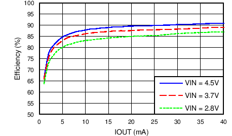
    • > 85% at IOUT > 10 mA
    • > 90% at IOUT > 40 mA
  • Excellent Performance
    • Outstanding Transient Response
    • 1% Output Voltage Accuracy over
      Full Temperature Range
  • I2C Interface
    • Programmable Power-Up / -Down
      Sequencing Options
    • Flexible Output Voltage Programming
    • Programmable Active Output Discharge
    • > 1000x Programmable Non-Volatile Memory
  • Under-Voltage Lock-Out and Thermal Protection
  • Two Package Options
    • 15-Ball CSP Package
    • 20-Pins QFN Package

Applications

  • Small-, Medium-Size Bipolar LCD Displays
    • Smartphone, Tablet
    • Camera, GPS
    • Home Automation, Point-of-Sales
    • Wearables (Smart Watch, Activity Tracker)
  • General Split-Rail Power Supply
    • Differential Audio, Headphone Amplifier
    • Instrumentation, Operational Amplifier, Comparator
    • DAC / ADC

Description

The TPS65132 family is designed to supply positive/negative driven applications. The device uses a single inductor scheme for both outputs to provide the user smallest solution size, a small bill-of-material as well as high efficiency. The devices offer best line and load regulation at low noise. With its input voltage range of 2.5 V to 5.5 V, it is optimized for products powered by single-cell batteries (Li-Ion, Ni-Li, Li-Polymer) and fixed 3.3-V and 5-V rails. The TPS656132 family provides 80 mA and 150 mA output current options with programmability to 40 mA. There are both CSP and QFN package options available.

Device Information (1)

PART NUMBER PACKAGE BODY SIZE (NOM.)
TPS65132
-B, -L, -T, -S
DSBGA (15) 2.11 mm × 1.51 mm
TPS65132W WQFN (20) 4.00 mm × 3.00 mm
  1. For all available packages, see the orderable addendum at the end of the datasheet.

space

space

Typical Application
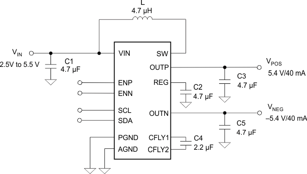
TPS65132 typ_app_slvsbm1.gif

Efficiency vs Output Current

TPS65132 C003_SLVSBM1.png