SLVAEW1 August 2020 – MONTH TPS63900 , TPS63901
Tech Note
The TPS63900 is a high-efficient synchronous buck-boost converter with an extremely low quiescent current (75 nA typical). The 2-level dynamic voltage-scaling feature lets applications switch between two output voltages during operation; for example, to save power by using a lower system supply voltage during standby operation. Some applications, for example, a headphone amplifier, might need additional voltage levels to finely adjust the amplifier output power for different headphone loads.
This application note describes options to implement multi-level digital voltage scaling with TPS63900.
CFG pin interface
The device has a three configuration pins (CFGx) with a resistor to digital (R2D) interface. One of 16 different resistor values select the settings on each CFGx pin (see data sheet for programming options). The three CFGx pins allow the user to program an optional input current limit and two output voltages (VO(1) and VO(2)), that are selectable via the SEL pin. The output voltage changes between the two targets with a slew rate of 100 mV in 125 μs or 0.8 V/ms (see Figure 1-1).
The device does not actively discharge the output capacitor, when the output voltage ramps from a high to a lower output voltage. This leads to a longer output voltage settling time when light load is applied (see Figure 1-2). The settling time can be calculated with Equation 1.
where
- tsettle is the capacitor discharge time
- VO(HIGH) is the higher output voltage
- VO(LOW) is the lower output voltage
- IO is the average output current
- CO is the effective output capacitance
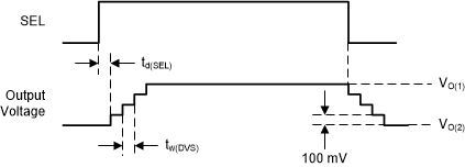 Figure 1-1 DVS with high load
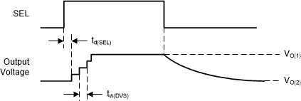 Figure 1-2 DVS with light load
Start-up behavior
During normal operation of the converter the R2D interface is disabled to save power and increase efficiency. The device evaluates the CFG pins only at startup after the EN pin toggles from low to high with Vin already applied (see Figure 1-3). The enable time from the EN low to high transition until the device starts operating is specified with maximum td(EN) = 1.5 ms. After this, the soft-start feature ramps up the output voltage (see data sheet for further details). The typical output voltage ramp time can be calculated with Equation 2.
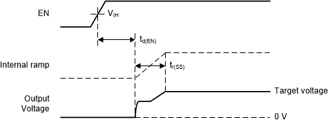 Figure 1-3 Start-up behavior
where
- tr(SS) is the rise time of the output voltage in ms
The total start-up time from the EN low to high transition until a settled output voltage is the sum of td(EN) and tr(SS).
The device can start-up, when the output voltage is not zero. This is beneficial, if the application requires an output voltage, when changing the CFG pin setting. However, in this case the output capacitor needs to be sized accordingly that it can supply the system during the td(EN) time. Equation 3 can be used to calculate the output capacitor size (CO).
where
- VO(HIGH) is the output voltage before the change
- VO(LOW) is the allowed minimum voltage
Re-read of CFG pins
One option is to change the resistor value on a CFG pin. A change of the resistor value on a CFG pin only changes the configuration after toggling the EN pin from high to low to high.
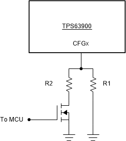 Figure 1-4 Multi resistor
configuration
Figure 1-4 Multi resistor
configurationFigure 1-4 shows a simple implementation to switch between 2 resistor values. R1 will be selected when the transistor is open. When the transistor is closed, the parallel resistance of both resistors determines the new value (Rtotal). R2 is the parallel resistor that can be calculated with Equation 4.
where
- Rtotal is the needed parallel resistance of R1 and R2 for the new setting
For example, if CFG3 setting should be changed between 2.1 V and 3.3 V, R1 has to be 16.2 kΩ. With R2 = 1.24 kΩ, Rtotal calculates to 1.152 kΩ.
Using a reference voltage
Instead of switching resistors, a voltage can be applied to the CFG pin. Figure 1-5 shows the internal structure of the R2D interface. At start-up the ADC reads the voltage across the external resistor. Therefore one can apply a voltage (VCFG) with a DAC to the CFG pin during start-up. After start-up the DAC can be disabled.
Note, the needed voltage depends on the input voltage (VIN) and the external resistor. The voltage can be calculated with Equation 5.
where
- Rint = 33 kΩ
- Rext is the desired configuration value
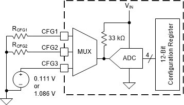 Figure 1-5 Internal structure of CFG pin
interface
Figure 1-5 Internal structure of CFG pin
interfaceFor example, if CFG3 setting should be changed between 2.1 V and 3.3 V setting at VIN = 3.3 V, VCFG is 111 mV or 1.086 V.