SLUSA44A March 2010 – July 2015 BQ24640
PRODUCTION DATA.
- 1 Features
- 2 Applications
- 3 Description
- 4 Revision History
- 5 Pin Configuration and Functions
- 6 Specifications
-
7 Detailed Description
- 7.1 Overview
- 7.2 Functional Block Diagram
- 7.3
Feature Description
- 7.3.1 Output Voltage Regulation
- 7.3.2 Output Current Regulation
- 7.3.3 Power Up
- 7.3.4 Enable and Disable Charging
- 7.3.5 Automatic Internal Soft-Start Charger Current
- 7.3.6 Converter Operation
- 7.3.7 Synchronous and Nonsynchronous Operation
- 7.3.8 Input Overvoltage Protection (ACOV)
- 7.3.9 Output Overvoltage Protection
- 7.3.10 Cycle-by-Cycle Charge Overcurrent Protection
- 7.3.11 Thermal Shutdown Protection
- 7.3.12 Temperature Qualification
- 7.3.13 CE (Charge Enable)
- 7.3.14 PG Output
- 7.3.15 Charge Status Outputs
- 7.4 Device Functional Modes
- 8 Application and Implementation
- 9 Power Supply Recommendations
- 10Layout
- 11Device and Documentation Support
- 12Mechanical, Packaging, and Orderable Information
1 Features
- Charge Super Capacitor Pack From 2.1 V to 26 V
- CC/CV Charge Profile From 0 V Without Precharge
- 600-kHz NMOS-NMOS Synchronous Buck Controller
- Over 90% Efficiency for up to 10-A Charge Current
- 5-V to 28-V VCC Input Voltage Range
- Accuracy
- ±0.5% Charge Voltage Regulation
- ±3% Charge Current Regulation
- High Integration
- Internal Loop Compensation
- Internal Digital Soft Start
- Safety
- Input Overvoltage Protection
- Capacitor Temperature Sensing Hot and Cold Charge Suspend
- Thermal Shutdown
- Status Outputs
- Adapter Present
- Charger Operation Status
- Charge Enable Pin
- 30-ns Driver Dead Time and 99.5% Maximum Effective Duty Cycle
- Automatic Sleep Mode for Low Power Consumption
- <15-µA Off-State Super Capacitor Discharge Current
- <1.5-mA Off-State Input Quiescent Current
2 Applications
- Memory Backup Systems
- Industrial UPS Systems and Power Transient Buffering
- Bridge Power to Buffer the Battery
3 Description
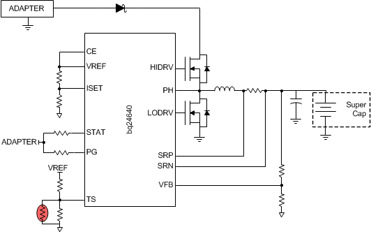
The bq24640 device is a highly integrated switched-mode super capacitor charge controller. The device offers a constant-frequency synchronous PWM controller with high accuracy charge current, voltage regulation, and charge status monitoring.
The bq24640 charges a super capacitor in two phases: constant current and constant voltage (CC/CV). The device can charge super capacitors from 0 V with current set on the ISET pin. When the super capacitor voltage reaches the programmed target voltage, charge current begins tapering down.
The bq24640 enters a low-current sleep mode
(<15 μA) when the input voltage falls below the output capacitor voltage.
The bq24640 has an input CE pin to enable and disable charge, and the STAT and PG output pins report charge and adapter status. The TS pin on the bq24640 monitors the temperature of the capacitor and suspends charge during hot and cold conditions.
Device Information(1)
| PART NUMBER | PACKAGE | BODY SIZE (NOM) |
|---|---|---|
| bq24640 | VQFN (16) | 3.50 mm × 3.50 mm |
- For all available packages, see the orderable addendum at the end of the data sheet.
Simplified Schematic
