SLLSEH9B October 2013 – July 2016 TPD1S414
PRODUCTION DATA.
- 1 Features
- 2 Applications
- 3 Description
- 4 Revision History
- 5 Pin Configuration and Functions
-
6 Specifications
- 6.1 Absolute Maximum Ratings
- 6.2 ESD Ratings
- 6.3 Recommended Operating Conditions
- 6.4 Thermal Information
- 6.5 Electrical Characteristics (EN, ACK Pins)
- 6.6 Electrical Characteristics (OVP Circuit)
- 6.7 Timing Requirements
- 6.8 Switching Characteristics (nFET)
- 6.9 Supply Current Consumption
- 6.10 Thermal Shutdown Feature
- 6.11 Typical Characteristics
-
7 Detailed Description
- 7.1 Overview
- 7.2 Functional Block Diagram
- 7.3
Feature Description
- 7.3.1 Overvoltage Protection on VBUS_CON up to 30-V DC
- 7.3.2 Low RON nFET Switch Supports Host and Charging Mode
- 7.3.3 ±15-kV IEC 61000-4-2 Level 4 ESD Protection
- 7.3.4 100-V IEC 61000-4-5 µs Surge Protection
- 7.3.5 Start-Up and OVP Recovery Delay
- 7.3.6 Integrated Input Enable and Status Output Signal
- 7.3.7 Thermal Shutdown
- 7.4 Device Functional Modes
- 8 Application and Implementation
- 9 Power Supply Recommendations
- 10Layout
- 11Device and Documentation Support
- 12Mechanical, Packaging, and Orderable Information
1 Features
- Overvoltage Protection at VBUS_CON Up to 30-V DC
- Low RON nFET Switch Supports Host and Charging Mode
- Internal 15-ms Start-Up Delay
- Internal 30-ms Soft-Start Delay to Minimize the USB Inrush Current
- Transient Protection for VBUS Line:
- IEC 61000-4-2 Contact Discharge ±15 kV
- IEC 61000-4-2 Air Gap Discharge ±15 kV
- IEC 61000-4-5 Open-Circuit Voltage 100 V
- Integrated Input Enable and Status Output Signal
- Thermal Shutdown (TSD) Feature
- Space-Saving DSBGA Package: (1.4 mm × 1.89 mm)
2 Applications
- End Equipment
- Mobile Phones
- Tablets
- Wearables
- Electronic-Point-of-Sale (EPOS)
- Interfaces
- USB 2.0
- USB 3.0
- USB Type C
3 Description
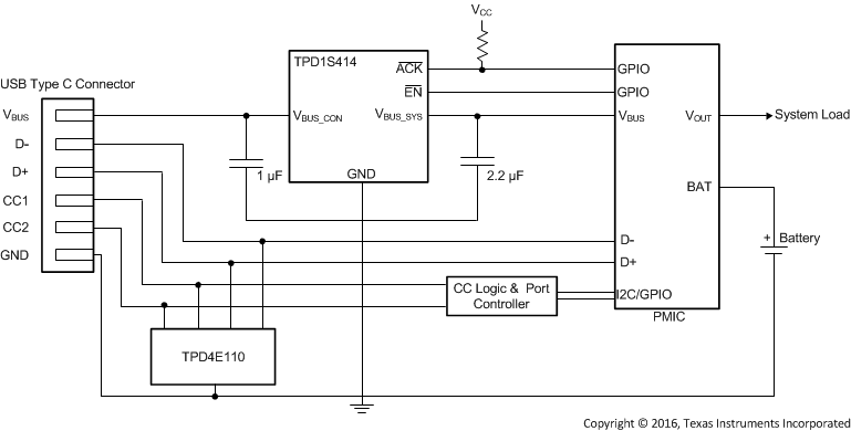
The TPD1S414 device is a single-chip solution for a USB connector’s VBUS line protection. The bidirectional nFET switch ensures safe current flow in both charging and host mode while protecting the internal system circuits from any overvoltage conditions at the VBUS_CON pin. On the VBUS_CON pin, this device can handle overvoltage protection up to 30 V. After the EN pin toggles low, the TPD1S414 waits 20 ms before turning ON the nFET through a soft-start delay. ACK pin indicates the FET is completely turned ON.
The typical application interface for the TPD1S414 is the VBUS line in USB connectors. Typical end equipment for TPD1S414 are mobiles phones, tablets, wearables, and electronic-point-of-sale (EPOS). The TPD1S414 can also be applied to any system using an interface with a 5-V power rail.
Device Information(1)
| PART NUMBER | PACKAGE | BODY SIZE (NOM) |
|---|---|---|
| TPD1S414 | DSBGA (12) | 1.40 mm × 1.89 mm |
- For all available packages, see the orderable addendum at the end of the data sheet.
Typical Application Schematic
