SBVS162B March 2011 – July 2015 TPS7A4001
PRODUCTION DATA.
- 1 Features
- 2 Applications
- 3 Description
- 4 Revision History
- 5 Pin Configuration and Functions
- 6 Specifications
- 7 Detailed Description
- 8 Application and Implementation
- 9 Power Supply Recommendations
- 10Layout
- 11Device and Documentation Support
- 12Mechanical, Packaging, and Orderable Information
1 Features
- Very High Maximum Input Voltage: 100 V
- Wide Input Voltage Range: 7 to 100 V
- Accuracy:
- Nominal: 1%
- Over Line, Load, and Temperature: 2.5%
- Low Quiescent Current: 25 µA
- Quiescent Current at Shutdown: 4.1 µA
- Maximum Output Current: 50 mA
- CMOS Logic-Level-Compatible Enable Pin
- Adjustable Output Voltage from about 1.175 to
90 V - Stable With Ceramic Capacitors:
- Input Capacitance: ≥1 µF
- Output Capacitance: ≥4.7 µF
- Dropout Voltage: 290 mV
- Built-In Current Limit and Thermal Shutdown Protection
- Package: High Thermal Performance HVSSOPPowerPAD™
- Operating Temperature Range: –40°C to 125°C
2 Applications
- Microprocessors, Microcontrollers Powered by Industrial Busses With High Voltage Transients
- Industrial Automation
- Telecom Infrastructure
- Automotive
- Power over Ethernet (PoE)
- LED Lighting
- Bias Power Supplies
3 Description
The TPS7A4001 device is a very high voltage-tolerant linear regulator that offers the benefits of a thermally-enhanced package (HVSSOP), and is able to withstand continuous DC or transient input voltages of up to 100 V.
The TPS7A4001 device is stable with any output capacitance greater than 4.7 µF and any input capacitance greater than 1 µF (over temperature and tolerance). Therefore, implementations of this device require minimal board space because of its miniaturized packaging (HVSSOP) and a potentially small output capacitor. In addition, the TPS7A4001 device offers an enable pin (EN) compatible with standard CMOS logic to enable a low-current shutdown mode.
The TPS7A4001 device has an internal thermal shutdown and current limiting to protect the system during fault conditions. The HVSSOP packages has an operating temperature range of TJ = –40°C to 125°C.
In addition, the TPS7A4001 device is ideal for generating a low-voltage supply from intermediate voltage rails in telecom and industrial applications; not only can it supply a well-regulated voltage rail, but it can also withstand and maintain regulation during very high and fast voltage transients. These features translate to simpler and more cost-effective electrical surge-protection circuitry for a wide range of applications, including PoE, bias supply, and LED lighting.
Device Information(1)
| PART NUMBER | PACKAGE | BODY SIZE (NOM) |
|---|---|---|
| TPS7A4001 | HVSSOP (8) | 3.00 mm × 5.00 mm |
- For all available packages, see the orderable addendum at the end of the data sheet.
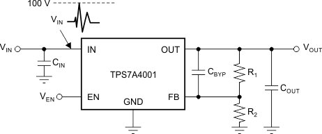
Typical Application Schematic
