SBOA425 February 2021 ADS8588S , ADS8688A , INA826
Application Brief
Introduction
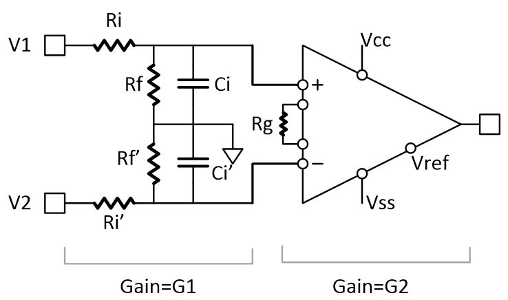
Supporting high-voltage common-mode input in the range of ±30 V is a common requirement for programmable logic controller (PLC) analog input modules. One way to support high-common mode is with signal passive scaling in front of instrumentational amplifier similar to the circuit shown in Figure 1-1.
 Figure 1-1 Passive scaling plus instrumentation
amplifier
Figure 1-1 Passive scaling plus instrumentation
amplifierAn instrumentation amplifier similar to INA826 can be used along with matched resistors. The gain of this circuit is represented as:


When examining the performance of this circuit with G1=0.249, and G2=4.01, for example, overall unity gain is achieved for the interface. These gains can be achieved with 0.1% standard resistors Rf=249 kΩ, Ri=750 kΩ, RG=16.4 kΩ.
Common-Mode Range
With the aforementioned values, input voltages of the amplifier are


Where Vi and VCMare the differential input and common-mode input voltages respectively.

If Vi range of ±10 V is assumed, we can determine the VCM range given the input voltages derived above. The instrumentational amplifier valid input range is complex to calculate, and depends on power supply levels and gain.
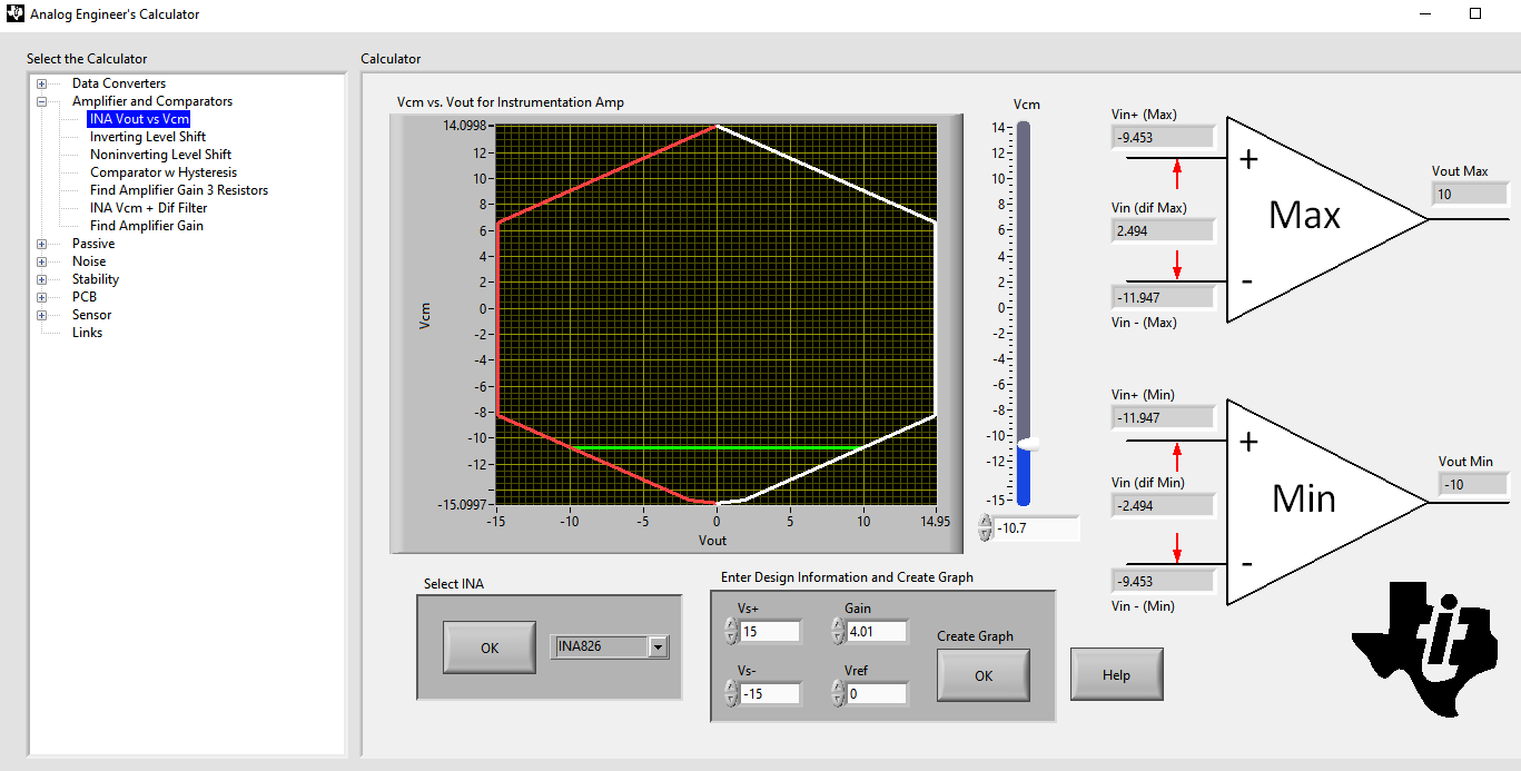
We can use Figure 1-2 function in TI's Analog engineer's calculator tool as shown in Figure 1-2 to quickly calculate the common-mode range assuming bipolar supply of ±15 V and Vref=0. Using the tool shows Vcm at the amplifier input limits are 9.05 V and -10.7 V, by calculating back the input terminal common-mode range we come to the following values: -42.9 V to +36.3 V
 Figure 1-2 Common-mode input range calculator for
instrumentation amplifiers
Figure 1-2 Common-mode input range calculator for
instrumentation amplifiersInput Impedance
Input impedance of the circuit in Figure 1-1 is:


With chosen resistor values, 1 MΩ, and 2 MΩ respectively.
Offset Error
While input impedance is determined only by font-end, both front-end and the ADC are affecting other parameters like offset and gain errors. Figure 1-3 shows the front-end connected to the simultaneous sampling ADS8588S. Figure 1-3 Front-end connected to
ADS8588S
Figure 1-3 Front-end connected to
ADS8588SUsing the sum of squares, we can calculate the overall offset of the signal chain at the input of the ADC as:

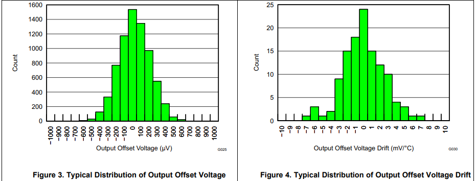
Where ADC offset is input-referred, and amplifier offset is output-referred. Both ADC and amplifier offsets and offset drifts are found in respective data sheets. Figure 1-4 shows the offset and offset drift distribution for INA826.
 Figure 1-4 Offset characteristics of
INA826
Figure 1-4 Offset characteristics of
INA826Initial offset can be eliminated using calibration, while offset drift contributes to uncompensated offset error over temperature. At low gains, output offset dominates the instrumentational amplifier offset. INA826 offset typical value is 200 µV, and drift value is about 2 µV/℃, this leads to ±0.12 mV over -40 ℃ to 85 ℃.
ADC8588S features a typical offset of 150 µV and a negligible offset drift of 0.3 ppm/℃. The applying offset equation above we get a typical RMS total offset of 250 µV and 2 µV/℃. It’s worth noting that worst-case offset values are way above this. However, the worst-case values are too pessimistic and typical values are much more realistic.
CM-related Offset Error
When CM voltage is added to a zero-input voltage, another component of offset is introduced due to the input resistors mismatch which is dependent on the common-mode gain.

Where ΔR/R is the resistor tolerance, and α is equals 4 in case of worst-case calculation, and 0.33 for the typical case. CM-induced offset error can be calculated by multiplying this gain by the common-mode range.

Gain Error
For the full chain, gain error consists of three components: resistors, amplifier, and ADC

The resistors gain error εG1 can be estimated using Monte-Carlo simulation based on the given resistor tolerance (0.1%). The simulation results show a three-sigma value of (0.125%). The amplifier typical intrinsic gain error is 0.03% according to data sheet, so the amplifier gain error will be dominated by gain setting resistor Rg tolerance (0.1%). The ADC typical gain error is ±4 LSB=0.01% which is negligible. Substituting these values, we get 0.16% as overall gain error. This translates to 16 mV gain error in case of 10 V input range.
In case of non-zero common mode, the CM-related offset error would appear as gain error, by adding both values, the full-scale error would be close to 19 mV or 0.19%.
Signal Bandwidth
The signal goes over three subsequent filters through the signal chain.
- The RC filter of the front-end.
- The bandwidth of the INA826.
- The bandwidth of the ADS8588S.
Combining these filters leads to an overall bandwidth of 21 kHz. This bandwidth will result in a 0.01% linear settling time of 70 µs.
- RC filter of 750 kΩ and 1pF differential input impedance has 212 kHz of bandwidth
- INA826 bandwidth is about 700 kHz
- ADS8588 has an integrated filter with 24-kHz bandwidth
Full-scale Error
At full-scale input, in addition to non-zero common-mode several errors are added to get the full-scale error.

Common-Mode Rejection Ratio
It can be proven that CMRR due to resistor mismatch (Rf and Rƒ, Rii and Ri’) equals:

Test Results
The analog signal chain shown in Figure 1-3 is put under test to validate calculations presented in this article. Note that some statistical parameters like offset error cannot be really validated using a single device sample.
| Parameter | Measured value | Unit |
|---|---|---|
| Vos | -0.35 | mV |
| Vos|cm (±20V) | 2.3 to 3.0 | mV |
| εG | ±0.01 | %FSR |
| εFS | -0.4 to +0.12 | %FSR |
| BW | 21.2 | kHz |
| tsettle | 155 | us |
| CMRR | 77 | dB |
| Cross talk | -48 | dB |
| 3rd HD | -109 | dB |
Table 1-1 shows the measured parameters of few input channels attached to one ADC. Measured results to a great extent matches our previous calculation. The settling time is higher than calculated probably due to non-linear settling effect. Gain error is also lower than calculated, which might be attributed to limited sampling. The techniques introduced in this document can also be applied to the instrumentation amplifiers listed in Table 1-2.
| Related devices | Description |
|---|---|
| INA818 | Low power (350 μA), high precision (35 μV), low noise 36 V instrumentation amp with over-voltage protection (gain pins 1, 8) |
| INA819 | Low power (350 μA), high precision (35 μV), low noise 36 V instrumentation amp with over-voltage protection (gain pins 2, 3)- Tiny 3x3mm package available |
| INA821 | Wide bandwidth (4.7 MHz), low noise (7 nV/√Hz), high precision (35 μV) 36 V instrumentation amp with over-voltage protection- Tiny 3x3mm package available |
| INA849 | Ultra-low noise (1 n/√Hz), high speed (35 V/μs, 28 MHz), high precision (35 μV) 36 V instrumentation amplifier. Fixed gain of 2,000 version available (INA848). |
| INA333 | Micro-power (50 μA), Zero-Drift (25 μV, 0.1 μV/⁰C), low voltage instrumentation amplifier. Tiny 3x3mm package available |
References
- Texas Instruments, Difference Amplifier (subcontractor) Circuit, Analog Engineer's Circuit: Amplifiers.
- Texas Instruments, 16-bit 8-Channel PLC Analog Input Module with High Voltage CM support, application brief.