SBAS535C August   2013  – February 2017 ADS1120

PRODUCTION DATA.  

  1. Features
  2. Applications
  3. Description
  4. Revision History
  5. Pin Configuration and Functions
  6. Specifications
    1. 6.1 Absolute Maximum Ratings
    2. 6.2 ESD Ratings
    3. 6.3 Recommended Operating Conditions
    4. 6.4 Thermal Information
    5. 6.5 Electrical Characteristics
    6. 6.6 SPI Timing Requirements
    7. 6.7 SPI Switching Characteristics
    8. 6.8 Typical Characteristics
  7. Parameter Measurement Information
    1. 7.1 Noise Performance
  8. Detailed Description
    1. 8.1 Overview
    2. 8.2 Functional Block Diagram
    3. 8.3 Feature Description
      1. 8.3.1  Multiplexer
      2. 8.3.2  Low-Noise PGA
        1. 8.3.2.1 PGA Common-Mode Voltage Requirements
        2. 8.3.2.2 Bypassing the PGA
      3. 8.3.3  Modulator
      4. 8.3.4  Digital Filter
      5. 8.3.5  Output Data Rate
      6. 8.3.6  Voltage Reference
      7. 8.3.7  Clock Source
      8. 8.3.8  Excitation Current Sources
      9. 8.3.9  Low-Side Power Switch
      10. 8.3.10 Sensor Detection
      11. 8.3.11 System Monitor
      12. 8.3.12 Offset Calibration
      13. 8.3.13 Temperature Sensor
        1. 8.3.13.1 Converting from Temperature to Digital Codes
          1. 8.3.13.1.1 For Positive Temperatures (for Example, 50°C):
          2. 8.3.13.1.2 For Negative Temperatures (for Example, -25°C):
        2. 8.3.13.2 Converting from Digital Codes to Temperature
    4. 8.4 Device Functional Modes
      1. 8.4.1 Power-Up and Reset
      2. 8.4.2 Conversion Modes
        1. 8.4.2.1 Single-Shot Mode
        2. 8.4.2.2 Continuous Conversion Mode
      3. 8.4.3 Operating Modes
        1. 8.4.3.1 Normal Mode
        2. 8.4.3.2 Duty-Cycle Mode
        3. 8.4.3.3 Turbo Mode
        4. 8.4.3.4 Power-Down Mode
    5. 8.5 Programming
      1. 8.5.1 Serial Interface
        1. 8.5.1.1 Chip Select (CS)
        2. 8.5.1.2 Serial Clock (SCLK)
        3. 8.5.1.3 Data Ready (DRDY)
        4. 8.5.1.4 Data Input (DIN)
        5. 8.5.1.5 Data Output and Data Ready (DOUT/DRDY)
        6. 8.5.1.6 SPI Timeout
      2. 8.5.2 Data Format
      3. 8.5.3 Commands
        1. 8.5.3.1 RESET (0000 011x)
        2. 8.5.3.2 START/SYNC (0000 100x)
        3. 8.5.3.3 POWERDOWN (0000 001x)
        4. 8.5.3.4 RDATA (0001 xxxx)
        5. 8.5.3.5 RREG (0010 rrnn)
        6. 8.5.3.6 WREG (0100 rrnn)
      4. 8.5.4 Reading Data
      5. 8.5.5 Sending Commands
      6. 8.5.6 Interfacing with Multiple Devices
    6. 8.6 Register Map
      1. 8.6.1 Configuration Registers
        1. 8.6.1.1 Configuration Register 0 (offset = 00h) [reset = 00h]
        2. 8.6.1.2 Configuration Register 1 (offset = 01h) [reset = 00h]
        3. 8.6.1.3 Configuration Register 2 (offset = 02h) [reset = 00h]
        4. 8.6.1.4 Configuration Register 3 (offset = 03h) [reset = 00h]
  9. Application and Implementation
    1. 9.1 Application Information
      1. 9.1.1 Serial Interface Connections
      2. 9.1.2 Analog Input Filtering
      3. 9.1.3 External Reference and Ratiometric Measurements
      4. 9.1.4 Establishing a Proper Common-Mode Input Voltage
      5. 9.1.5 Unused Inputs and Outputs
      6. 9.1.6 Pseudo Code Example
    2. 9.2 Typical Applications
      1. 9.2.1 K-Type Thermocouple Measurement (-200°C to +1250°C)
        1. 9.2.1.1 Design Requirements
        2. 9.2.1.2 Detailed Design Procedure
        3. 9.2.1.3 Application Curves
      2. 9.2.2 3-Wire RTD Measurement (-200°C to +850°C)
        1. 9.2.2.1 Design Requirements
        2. 9.2.2.2 Detailed Design Procedure
          1. 9.2.2.2.1 Design Variations for 2-Wire and 4-Wire RTD Measurements
        3. 9.2.2.3 Application Curves
      3. 9.2.3 Resistive Bridge Measurement
        1. 9.2.3.1 Design Requirements
        2. 9.2.3.2 Detailed Design Procedure
  10. 10Power Supply Recommendations
    1. 10.1 Power-Supply Sequencing
    2. 10.2 Power-Supply Ramp Rate
    3. 10.3 Power-Supply Decoupling
  11. 11Layout
    1. 11.1 Layout Guidelines
    2. 11.2 Layout Example
  12. 12Device and Documentation Support
    1. 12.1 Documentation Support
      1. 12.1.1 Related Documentation
    2. 12.2 Receiving Notification of Documentation Updates
    3. 12.3 Community Resources
    4. 12.4 Trademarks
    5. 12.5 Electrostatic Discharge Caution
    6. 12.6 Glossary
  13. 13Mechanical, Packaging, and Orderable Information

Features

  • Low Current Consumption:
    As Low as 120 μA (typ) in Duty-Cycle Mode
  • Wide Supply Range: 2.3 V to 5.5 V
  • Programmable Gain: 1 V/V to 128 V/V
  • Programmable Data Rates: Up to 2 kSPS
  • 16-Bit Noise-Free Resolution at 20 SPS
  • Simultaneous 50-Hz and 60-Hz Rejection at
    20 SPS with Single-Cycle Settling Digital Filter
  • Two Differential or Four Single-Ended Inputs
  • Dual-Matched Programmable Current Sources:
    50 μA to 1.5 mA
  • Internal 2.048-V Reference: 5 ppm/°C (typ) Drift
  • Internal 2% Accurate Oscillator
  • Internal Temperature Sensor:
    0.5°C (typ) Accuracy
  • SPI-Compatible Interface (Mode 1)
  • Package: 3.5-mm × 3.5-mm × 0.9-mm VQFN

Applications

  • Temperature Sensor Measurements:
    • Thermistors
    • Thermocouples
    • Resistance Temperature Detectors (RTDs):
      2-, 3-, or 4-Wire Types
  • Resistive Bridge Sensor Measurements:
    • Pressure Sensors
    • Strain Gauges
    • Weigh Scales
  • Portable Instrumentation
  • Factory Automation and Process Controls

Description

The ADS1120 is a precision, 16-bit, analog-to-digital converter (ADC) that offers many integrated features to reduce system cost and component count in applications measuring small sensor signals. The device features two differential or four single-ended inputs through a flexible input multiplexer (MUX), a low-noise, programmable gain amplifier (PGA), two programmable excitation current sources, a voltage reference, an oscillator, a low-side switch, and a precision temperature sensor.

The device can perform conversions at data rates up to 2000 samples-per-second (SPS) with single-cycle settling. At 20 SPS, the digital filter offers simultaneous 50-Hz and 60-Hz rejection for noisy industrial applications. The internal PGA offers gains up to 128 V/V. This PGA makes the ADS1120 ideally-suited for applications measuring small sensor signals, such as resistance temperature detectors (RTDs), thermocouples, thermistors, and bridge sensors. The device supports measurements of pseudo- or fully-differential signals when using the PGA. Alternatively, the device can be configured to bypass the internal PGA while still providing high input impedance and gains up to 4 V/V, allowing for single-ended measurements.

Power consumption is as low as 120 µA when operating in duty-cycle mode with the PGA disabled. The ADS1120 is offered in a leadless VQFN-16 or a TSSOP-16 package and is specified over a temperature range of –40°C to +125°C.

Device Information(1)

PART NUMBER PACKAGE BODY SIZE (NOM)
ADS1120 VQFN (16) 3.50 mm × 3.50 mm
TSSOP (16) 5.00 mm × 4.40 mm
  1. For all available packages, see the orderable addendum at the end of the datasheet.
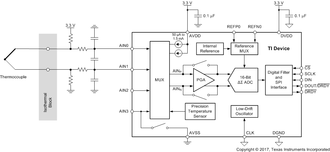
K-Type Thermocouple Measurement

ADS1120 FP_TC_example_bas535.gif