SLUSCE4A January 2017 – July 2017 TPS548B22
PRODUCTION DATA.
- 1 Features
- 2 Applications
- 3 Description
- 4 Revision History
- 5 Pin Configuration and Functions
- 6 Specifications
-
7 Detailed Description
- 7.1 Overview
- 7.2 Functional Block Diagram
- 7.3 Feature Description
- 7.4 Device Functional Modes
- 7.5 Programming
-
8 Applications and Implementation
- 8.1 Application Information
- 8.2
Typical Applications
- 8.2.1 TPS548B22 1.5-V to 18-V Input, 1-V Output, 25-A Converter
- 8.2.2 Design Requirements
- 8.2.3
Design Procedure
- 8.2.3.1 Switching Frequency Selection
- 8.2.3.2 Inductor Selection
- 8.2.3.3 Output Capacitor Selection
- 8.2.3.4 Input Capacitor Selection
- 8.2.3.5 Bootstrap Capacitor Selection
- 8.2.3.6 BP Pin
- 8.2.3.7 R-C Snubber and VIN Pin High-Frequency Bypass
- 8.2.3.8 Optimize Reference Voltage (VSEL)
- 8.2.3.9 MODE Pin Selection
- 8.2.3.10 Overcurrent Limit Design.
- 8.2.4 Application Curves
- 9 Power Supply Recommendations
- 10Layout
- 11Device and Documentation Support
- 12Mechanical, Packaging, and Orderable Information
パッケージ・オプション
デバイスごとのパッケージ図は、PDF版データシートをご参照ください。
メカニカル・データ(パッケージ|ピン)
- RVF|40
サーマルパッド・メカニカル・データ
- RVF|40
発注情報
1 Features
- Conversion Input Voltage Range (PVIN): 1.5 V to 18 V
- Input Bias Voltage (VDD) Range: 4.5 V to 22 V
- Output Voltage Range: 0.6 V to 5.5 V
- Integrated, 4.1-mΩ and 1.9-mΩ Power MOSFETs With 25-A Continuous Output Current
- Voltage Reference 0.6 V to 1.2 V in 50-mV Steps Using VSEL Pin
- ±0.5%, 0.9-VREF Tolerance Range: –40°C to +125°C Junction Temperature
- True Differential Remote Sense Amplifier
- D-CAP3™ Control Loop to Support Large Bulk Capacitors and/or Small MLCCs Without External Compensation
- Adaptive On-Time Control With 4 Selectable Frequency Settings: 425 kHz, 650 kHz, 875 kHz and 1.05 MHz
- Temperature Compensated and with Programmable Positive and Negative Current Limit and OC Clamp
- Choice of Hiccup or Latch-Off OVP or UVP
- VDD UVLO External Adjustment by Precision EN Hysteresis
- Prebias Start-up Support
- Eco-Mode and FCCM Selectable
- Full Suite of Fault Protection and PGOOD
- 7 mm × 5 mm × 1.5 mm, 40-Pin, Stack Clipped LQFN-CLIP Package
2 Applications
- Enterprise Storage, SSD, NAS
- Wireless and Wired Communication Infrastructure
- Industrial PCs, Automation, ATE, PLC, Video Surveillance
- Enterprise Server, Switches, Routers
- AISIC, SoC, FPGA, DSP Core and I/O Rails
3 Description
The TPS548B22 device is a compact single buck converter with adaptive on-time, D-CAP3 mode control. It is designed for high accuracy, high efficiency, fast transient response, ease-of-use, low external component count, and space-conscious power systems.
This device features full differential sense, TI integrated FETs with a high-side on-resistance of 4.1 mΩ and a low-side on-resistance of 1.9 mΩ. The device also features accurate 0.5%, 0.9-V reference with an ambient temperature range between –40°C and +125°C. Competitive features include: very low external component count, accurate load regulation and line regulation, output voltage setpoint accuracy, auto-skip or FCCM mode operation, and internal soft-start control.
The TPS548B22 device is available in 7 mm × 5 mm, 40-pin, LQFN-CLIP (RVF) package (RoHs exempt).
Device Information(1)
| PART NUMBER | PACKAGE | BODY SIZE (NOM) |
|---|---|---|
| TPS548B22 | LQFN-CLIP (40) | 7.00 mm × 5.00 mm |
- For all available packages, see the orderable addendum at the end of the data sheet.
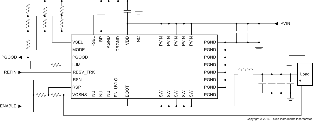
Simplified Application
