SNAS654A March 2015 – July 2016 LMX2571
PRODUCTION DATA.
- 1 Features
- 2 Applications
- 3 Description
- 4 Revision History
- 5 Pin Configuration and Functions
- 6 Specifications
-
7 Detailed Description
- 7.1 Overview
- 7.2 Functional Block Diagram
- 7.3
Feature Description
- 7.3.1 Reference Oscillator Input
- 7.3.2 R-Dividers and Multiplier
- 7.3.3 PLL Phase Detector and Charge Pump
- 7.3.4 PLL N-Divider and Fractional Circuitry
- 7.3.5 Partially Integrated Loop Filter
- 7.3.6 Low-Noise, Fully Integrated VCO
- 7.3.7 External VCO Support
- 7.3.8 Programmable RF Output Divider
- 7.3.9 Programmable RF Output Buffer
- 7.3.10 Integrated TX, RX Switch
- 7.3.11 Powerdown
- 7.3.12 Lock Detect
- 7.3.13 FSK Modulation
- 7.3.14 FastLock
- 7.3.15 Register Readback
- 7.4 Device Functional Modes
- 7.5 Programming
- 7.6
Register Maps
- 7.6.1 R60 Register (offset = 3Ch) [reset = 4000h]
- 7.6.2 R58 Register (offset = 3Ah) [reset = C00h]
- 7.6.3 R53 Register (offset = 35h) [reset = 2802h]
- 7.6.4 R47 Register (offset = 2Fh) [reset = 0h]
- 7.6.5 R46 Register (offset = 2Eh) [reset = 1Ah]
- 7.6.6 R42 Register (offset = 2Ah) [reset = 210h]
- 7.6.7 R41 Register (offset = 29h) [reset = 810h]
- 7.6.8 R40 Register (offset = 28h) [reset = 101Ch]
- 7.6.9 R39 Register (offset = 27h) [reset = 11F0h]
- 7.6.10 R35 Register (offset = 23h) [reset = 647h]
- 7.6.11 R34 Register (offset = 22h) [reset = 1000h]
- 7.6.12 R33 Register (offset = 21h) [reset = 0h]
- 7.6.13 R25 to R32 Register (offset = 19h to 20h) [reset = 0h]
- 7.6.14 R24 Register (offset = 18h) [reset = 10h]
- 7.6.15 R23 Register (offset = 17h) [reset = 10A4h]
- 7.6.16 R22 Register (offset = 16h) [reset = 8584h]
- 7.6.17 R21 Register (offset = 15h) [reset = 101h]
- 7.6.18 R20 Register (offset = 14h) [reset = 28h]
- 7.6.19 R19 Register (offset = 13h) [reset = 0h]
- 7.6.20 R18 Register (offset = 12h) [reset = 0h]
- 7.6.21 R17 Register (offset = 11h) [reset = 0h]
- 7.6.22 R9 to R16 Register (offset = 9h to 10h) [reset = 0h]
- 7.6.23 R8 Register (offset = 8h) [reset = 10h]
- 7.6.24 R7 Register (offset = 7h) [reset = 10A4h]
- 7.6.25 R6 Register (offset = 6h) [reset = 8584h]
- 7.6.26 R5 Register (offset = 5h) [reset = 101h]
- 7.6.27 R4 Register (offset = 4h) [reset = 28h]
- 7.6.28 R3 Register (offset = 3h) [reset = 0h]
- 7.6.29 R2 Register (offset = 2h) [reset = 0h]
- 7.6.30 R1 Register (offset = 1h) [reset = 0h]
- 7.6.31 R0 Register (offset = 0h) [reset = 3h]
-
8 Application and Implementation
- 8.1
Application Information
- 8.1.1 Direct Digital FSK Modulation
- 8.1.2 Frequency and Output Port Switching with TrCtl Pin
- 8.1.3 OSCin Configuration
- 8.1.4 Register R0 F1F2_INIT, F1F2_MODE usage
- 8.1.5 FastLock with External VCO
- 8.1.6 OSCin Slew Rate
- 8.1.7 RF Output Buffer Power Control
- 8.1.8 RF Output Buffer Type
- 8.1.9 MULT Multiplier
- 8.1.10 Integrated VCO
- 8.2 Typical Applications
- 8.3 Do's and Don'ts
- 8.1
Application Information
- 9 Power Supply Recommendations
- 10Layout
- 11Device and Documentation Support
- 12Mechanical, Packaging, and Orderable Information
パッケージ・オプション
デバイスごとのパッケージ図は、PDF版データシートをご参照ください。
メカニカル・データ(パッケージ|ピン)
- NJK|36
サーマルパッド・メカニカル・データ
発注情報
1 Features
- Any Frequency from 10 MHz to 1344 MHz
- Low Phase Noise and Spurs
- –123 dBc/Hz at 12.5 kHz Offset at 480 MHz
- –145 dBc/Hz at 1 MHz Offset at 480 MHz
- Normalized PLL Noise Floor of –231 dBc/Hz
- Spurious Better Than –75 dBc/Hz
- New FastLock to Reduce Lock Time
- A Novel Technique to Remove Integer Boundary Spurs
- Integrated 5-V Charge Pump and Output Divider for External VCO Operation
- 2-, 4- and 8-Level or Arbitrary Level Direct Digital FSK Modulation
- One TX/RX Output or Two Fanout Outputs
- Crystal, XO or Differential Reference Clock Input
- Low Current Consumption
- 39-mA Typical Synthesizer Mode (Internal VCO)
- 9-mA Typical PLL Mode (External VCO)
- 24-Bit Fractional-N Delta Sigma Modulator
2 Applications
- Duplex Mode Digital Professional 2-Way Radio
- dPMR, DMR, PDT, P25 Phase I
- Low Power Radio Communication Systems
- Satcom Modem
- Wireless Microphone
- Propriety Wireless Connectivity
- Handheld Test and Measurement Equipment
3 Description
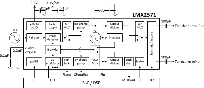
The LMX2571 is a low-power, high-performance, wideband PLLatinum™ RF synthesizer that integrates a delta-sigma fractional N PLL, multiple core voltage-controlled oscillator (VCO), programmable output dividers and two output buffers. The VCO cores work up to 5.376 GHz resulting in continuous output frequency range of 10 MHz to 1344 MHz.
This synthesizer can also be used with an external VCO. To that end, a dedicated 5-V charge pump and an output divider are available for this configuration.
A unique programmable multiplier is also incorporated to help improve spurs, allowing the system to use every channel even if it falls on an integer boundary.
The output has an integrated SPDT switch that can be used as a transmit/receive switch in FDD radio application. Both outputs can also be turned on to provide 2 outputs at the same time.
The LMX2571 supports direct digital FSK modulation through programming or pins. Discrete level FSK, pulse shaping FSK, and analog FM modulation are supported.
A new FastLock technique can be used allowing the user to step from one frequency to the next in less than 1.5 ms even when an external VCO is used with a narrow band loop filter.
Device Information(1)
| PART NUMBER | PACKAGE | BODY SIZE (NOM) |
|---|---|---|
| LMX2571 | WQFN (36) | 6.00 mm × 6.00 mm |
- For all available packages, see the orderable addendum at the end of the datasheet.
Simplified Schematic
