SNAS576D February 2012 – March 2016 LMK00308
PRODUCTION DATA.
- 1 Features
- 2 Applications
- 3 Description
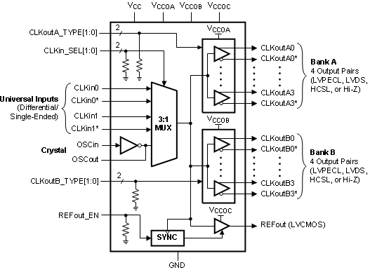
- 4 Functional Block Diagram
- 5 Revision History
- 6 Pin Configuration and Functions
- 7 Specifications
- 8 Parameter Measurement Information
- 9 Detailed Description
- 10Application and Implementation
- 11Power Supply Recommendations
- 12Device and Documentation Support
- 13Mechanical, Packaging, and Orderable Information
パッケージ・オプション
デバイスごとのパッケージ図は、PDF版データシートをご参照ください。
メカニカル・データ(パッケージ|ピン)
- RTA|40
サーマルパッド・メカニカル・データ
- RTA|40
発注情報
1 Features
- 3:1 Input Multiplexer:
- Two Universal Inputs Operate up to 3.1 GHz and Accept LVPECL, LVDS, CML, SSTL, HSTL, HCSL, or Single-Ended Clocks
- One Crystal Input Accepts a 10 to 40 MHz Crystal or Single-Ended Clock
- Two Banks with 4 Differential Outputs Each:
- LVPECL, LVDS, HCSL, or Hi-Z (Selectable Per Bank)
- LVPECL Additive Jitter with LMK03806 Clock Source at 156.25 MHz:
- 20 fs RMS (10 kHz to 1 MHz)
- 51 fs RMS (12 kHz to 20 MHz)
- High PSRR: -65 / -76 dBc (LVPECL/LVDS) at 156.25 MHz
- LVCMOS Output with Synchronous Enable Input
- Pin-Controlled Configuration
- VCC Core Supply: 3.3 V ± 5%
- 3 Independent VCCO Output Supplies: 3.3 V/2.5 V ± 5%
- Industrial Temperature Range: -40°C to +85°C
- 40-lead WQFN (6 mm × 6 mm)
2 Applications
3 Description
The LMK00308 is a 3-GHz, 8-output differential fanout buffer intended for high-frequency, low-jitter clock/data distribution and level translation. The input clock can be selected from two universal inputs or one crystal input. The selected input clock is distributed to two banks of 4 differential outputs and one LVCMOS output. Both differential output banks can be independently configured as LVPECL, LVDS, or HCSL drivers, or disabled. The LVCMOS output has a synchronous enable input for runt-pulse-free operation when enabled or disabled. The LMK00308 operates from a 3.3 V core supply and 3 independent 3.3 V/2.5 V output supplies.
The LMK00308 provides high performance, versatility, and power efficiency, making it ideal for replacing fixed-output buffer devices while increasing timing margin in the system.
Device Information(1)
| PART NUMBER | PACKAGE | BODY SIZE (NOM) |
|---|---|---|
| LMK00308 | WQFN (40) | 6.00 mm × 6.00 mm |
- For all available packages, see the orderable addendum at the end of the data sheet.
4 Functional Block Diagram

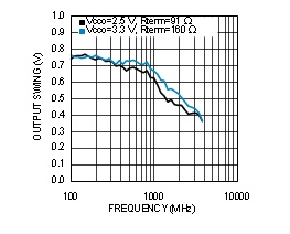
LVPECL Output Swing (VOD) vs. Frequency
