SLUSA49C April 2010 – June 2015
PRODUCTION DATA.
- 1 Features
- 2 Applications
- 3 Description
- 4 Revision History
- 5 Device Comparison Table
- 6 Pin Configuration and Functions
- 7 Specifications
-
8 Detailed Description
- 8.1 Overview
- 8.2 Functional Block Diagram
- 8.3
Feature Description
- 8.3.1 Battery Voltage Regulation
- 8.3.2 Battery Current Regulation
- 8.3.3 Input Adapter Current Regulation
- 8.3.4 Precharge
- 8.3.5 Charge Termination, Recharge, and Safety Timer
- 8.3.6 Power Up
- 8.3.7 Enable and Disable Charging
- 8.3.8 System Power Selector
- 8.3.9 Automatic Internal Soft-Start Charger Current
- 8.3.10 Converter Operation
- 8.3.11 Synchronous and Nonsynchronous Operation
- 8.3.12 Cycle-by-Cycle Charge Undercurrent Protection
- 8.3.13 Input Overvoltage Protection (ACOV)
- 8.3.14 Input Undervoltage Lockout (UVLO)
- 8.3.15 Battery Overvoltage Protection
- 8.3.16 Cycle-by-Cycle Charge Overcurrent Protection
- 8.3.17 Thermal Shutdown Protection
- 8.3.18 Temperature Qualification and JEITA Guideline
- 8.3.19 Timer Fault Recovery
- 8.3.20 PG Output
- 8.3.21 CE (Charge Enable)
- 8.3.22 Charge Status Outputs
- 8.3.23 Battery Detection
- 8.4 Device Functional Modes
- 9 Application and Implementation
- 10Power Supply Recommendations
- 11Layout
- 12Device and Documentation Support
- 13Mechanical, Packaging, and Orderable Information
1 Features
- Battery Thermistor Sense for JEITA Guideline Compatible Charger
- 600-kHz NMOS-NMOS Synchronous Buck Converter
- Stand-Alone Charger Support for Li-Ion or Li-Polymer
- 5-V–28-V VCC Input Operating Range and Supports 1 to 6 Battery Cells
- Up to 10-A Charge Current and Adapter Current
- High-Accuracy Voltage and Current Regulation
- ±0.5% Charge Voltage Accuracy
- ±3% Charge Current Accuracy
- ±3% Adapter Current Accuracy
- Integration
- Automatic System Power Selection From Adapter or Battery
- Internal Loop Compensation
- Internal Soft-Start
- Dynamic Power Management
- Safety Protection
- Input Overvoltage Protection
- Battery Detection
- Reverse Protection Input FET
- Programmable Safety Timer
- Charge Overcurrent Protection
- Battery Short Protection
- Battery Overvoltage Protection
- Thermal Shutdown
- Status Outputs
- Adapter Present
- Charger Operation Status
- Charge Enable Pin
- 6-V Gate Drive for Synchronous Buck Converter
- 30-ns Driver Dead-Time and 99.5% Maximum Effective Duty Cycle
- 24-Pin, 4-mm × 4-mm QFN Package
- Energy Star Low Quiescent Current Iq
- < 15-µA Off-State Battery Discharge Current
- < 1.5-mA Off-State Input Quiescent Current
2 Applications
- Netbooks, Mobile Internet Devices, and Ultra-Mobile PCs
- Industrial and Medical Equipment
- Personal Digital Assistants
- Handheld Terminals
- Portable Equipment
3 Description
The bq2461x device is a highly integrated, Japan Electronic Information Technology Association (JEITA) guideline-compatible, Li-ion or Li-polymer switched-mode battery charge controller. The device offers a constant-frequency synchronous switching PWM controller with high-accuracy charge current and voltage regulation, charge preconditioning, termination, adapter current regulation, and charge status monitoring
The bq2461x charges the battery in three phases: preconditioning, constant current, and constant voltage. Charge is terminated when the current reaches a minimum user-selectable level. A programmable charge timer provides a safety backup. The bq2461x automatically restarts the charge cycle if the battery voltage falls below an internal threshold, and enters a low quiescent current sleep mode when the input voltage falls below the battery voltage.
Device Information(1)
| PART NUMBER | PACKAGE | BODY SIZE (NOM) |
|---|---|---|
| bq24616 | VQFN (24) | 4.00 mm × 4.00 mm |
- For all available packages, see the orderable addendum at the end of the data sheet.
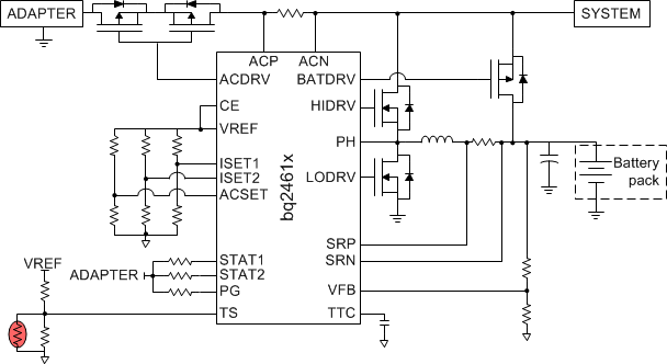
Typical Application Schematic

4 Revision History
Changes from B Revision (October 2011) to C Revision
- Added ESD Ratings table, Feature Description section, Device Functional Modes, Application and Implementation section, Power Supply Recommendations section, Layout section, Device and Documentation Support section, and Mechanical, Packaging, and Orderable Information sectionGo
Changes from A Revision (May 2010) to B Revision