SLLSEK5B July 2015 – May 2017 ISO7340-Q1 , ISO7341-Q1 , ISO7342-Q1
PRODUCTION DATA.
- 1 Features
- 2 Applications
- 3 Description
- 4 Revision History
- 5 Description (continued)
- 6 Pin Configuration and Functions
-
7 Specifications
- 7.1 Absolute Maximum Ratings
- 7.2 ESD Ratings
- 7.3 Recommended Operating Conditions
- 7.4 Thermal Information
- 7.5 Power Ratings
- 7.6 Insulation Specifications
- 7.7 Safety-Related Certifications
- 7.8 Safety Limiting Values
- 7.9 Electrical Characteristics—5-V Supply
- 7.10 Supply Current Characteristics—5-V Supply
- 7.11 Electrical Characteristics—3.3-V Supply
- 7.12 Supply Current Characteristics—3.3-V Supply
- 7.13 Switching Characteristics—5-V Supply
- 7.14 Switching Characteristics—3.3-V Supply
- 7.15 Insulation Characteristics Curves
- 7.16 Typical Characteristics
- 8 Parameter Measurement Information
- 9 Detailed Description
- 10Application and Implementation
- 11Power Supply Recommendations
- 12Layout
- 13Device and Documentation Support
- 14Mechanical, Packaging, and Orderable Information
Package Options
Refer to the PDF data sheet for device specific package drawings
Mechanical Data (Package|Pins)
- DW|16
Thermal pad, mechanical data (Package|Pins)
Orderable Information
1 Features
- Qualified for Automotive Applications
- AEC-Q100 Qualified With the Following Results:
- Device Temperature Grade 1: –40°C to 125°C Ambient Operating Temperature Range
- Device HBM Classification Level 3A
- Device CDM Classification Level C6
- Signaling Rate: 25 Mbps
- Integrated Noise Filter on the Inputs
- Default Output High and Low Options
- Low Power Consumption, Typical ICC per Channel at 1 Mbps:
-
ISO7340-Q1: 0.9 mA (5-V Supplies),
0.7 mA (3.3-V Supplies) -
ISO7341-Q1: 1.2 mA (5-V Supplies),
0.9 mA (3.3-V Supplies) -
ISO7342-Q1: 1.3 mA (5-V Supplies),
0.9 mA (3.3-V Supplies)
-
ISO7340-Q1: 0.9 mA (5-V Supplies),
- Low Propagation Delay: 31 ns
Typical (5-V Supplies) - 3.3-V and 5-V Level Translation
- 70-KV/μs Transient Immunity, Typical (5-V Supplies)
- Robust Electromagnetic Compatibility (EMC)
- System-level ESD, EFT, and Surge Immunity
- Low Emissions
- Operates from 3.3-V and 5-V Supplies
- Wide-Body SOIC-16 Package
- Safety-Related Certifications:
2 Applications
- Optocoupler Replacement in:
- Industrial Fieldbus
- Profibus
- Modbus
- DeviceNet Data Buses
- Servo Control Interface
- Motor Control
- Power Supplies
- Battery Packs
- Industrial Fieldbus
3 Description
The ISO734x-Q1 family of devices provides galvanic isolation up to 3000 VRMS for 1 minute per UL 1577 and 4242 VPK per VDE V 0884-10. These devices have four isolated channels comprised of logic input and output buffers separated by a silicon dioxide (SiO2) insulation barrier.
The ISO7340-Q1 device has four channels in forward direction, the ISO7341-Q1 device has three forward and one reverse-direction channels, and the ISO7342-Q1 device has two forward and two reverse-direction channels. In case of input power or signal loss, the default output is low for orderable part numbers with suffix F and high for orderable part numbers without suffix F. See the Device Functional Modes section for further details.
Device Information(1)
| PART NUMBER | PACKAGE | BODY SIZE |
|---|---|---|
| ISO7340-Q1 | SOIC (16) | 10.30 mm × 7.50 mm |
| ISO7341-Q1 | ||
| ISO7342-Q1 |
- For all available packages, see the orderable addendum at the end of the datasheet.
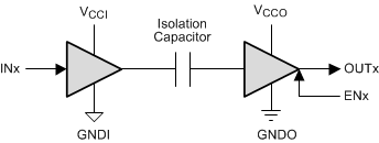
Simplified Schematic

4 Revision History
Changes from A Revision (August 2016) to B Revision
- Deleted Reinforced from the data sheet titleGo
Changes from * Revision (July 2016) to A Revision
- CQC certification is now certified instead of plannedGo
- Changed the minimum air gap (clearance) parameter (L(I01)) to the external clearance parameterGo
- Changed the minimum external tracking (creepage) parameter (L(I02)) to the external creepage parameterGo
- Changed the input-to-output test voltage parameter (VPR) to the apparent charge parameter (qpd)Go
- Changed the typ value for the enable propagation delay, high impedance-to-high output parameter of the FC devices and the typ value for the enable propagation delay, high impedance-to-low output parameter of the C devices from 16 to 16000 in the Switching Characteristics—3.3-V Supply tableGo
- Added the Receiving Notification of Documentation Updates section Go