SBOS485C November   2009  – May 2015 INA282 , INA283 , INA284 , INA285 , INA286

PRODUCTION DATA.  

  1. Features
  2. Applications
  3. Description
  4. Revision History
  5. Pin Configuration and Functions
  6. Specifications
    1. 6.1 Absolute Maximum Ratings
    2. 6.2 ESD Ratings
    3. 6.3 Recommended Operating Conditions
    4. 6.4 Thermal Information
    5. 6.5 Electrical Characteristics
    6. 6.6 Typical Characteristics
  7. Detailed Description
    1. 7.1 Overview
    2. 7.2 Functional Block Diagram
    3. 7.3 Feature Description
      1. 7.3.1 Selecting RS
      2. 7.3.2 Effective Bandwidth
      3. 7.3.3 Transient Protection
    4. 7.4 Device Functional Modes
      1. 7.4.1 Reference Pin Connection Options
        1. 7.4.1.1 Unidirectional Operation
          1. 7.4.1.1.1 Ground Referenced Output
          2. 7.4.1.1.2 V+ Referenced Output
        2. 7.4.1.2 Bidirectional Operation
          1. 7.4.1.2.1 External Reference Output
          2. 7.4.1.2.2 Splitting The Supply
          3. 7.4.1.2.3 Splitting an External Reference
      2. 7.4.2 Shutdown
      3. 7.4.3 Extended Negative Common-Mode Range
      4. 7.4.4 Calculating Total Error
        1. 7.4.4.1 Example 1
        2. 7.4.4.2 Example 2
  8. Applications and Implementation
    1. 8.1 Application Information
      1. 8.1.1 Basic Connections
    2. 8.2 Typical Applications
      1. 8.2.1 Current Summing
        1. 8.2.1.1 Design Requirements
        2. 8.2.1.2 Detailed Design Procedure
        3. 8.2.1.3 Application Curves
      2. 8.2.2 Current Differencing
        1. 8.2.2.1 Design Requirements
        2. 8.2.2.2 Detailed Design Procedure
        3. 8.2.2.3 Application Curves
  9. Power Supply Recommendations
  10. 10Layout
    1. 10.1 Layout Guidelines
    2. 10.2 Layout Example
  11. 11Device and Documentation Support
    1. 11.1 Related Links
    2. 11.2 Community Resources
    3. 11.3 Trademarks
    4. 11.4 Electrostatic Discharge Caution
    5. 11.5 Glossary
  12. 12Mechanical, Packaging, and Orderable Information

Package Options

Mechanical Data (Package|Pins)
Thermal pad, mechanical data (Package|Pins)
Orderable Information

1 Features

  • Wide Common-Mode Range: –14 V to +80 V
  • Offset Voltage: ±20 μV
  • CMRR: 140 dB
  • Accuracy:
    • ±1.4% Gain Error (Max)
    • 0.3 μV/°C Offset Drift
    • 0.005%/°C Gain Drift (Max)
  • Available Gains:
    • 50 V/V: INA282
    • 100 V/V: INA286
    • 200 V/V: INA283
    • 500 V/V: INA284
    • 1000 V/V: INA285
  • Quiescent Current: 900 μA (Max)

2 Applications

  • Telecom Equipment
  • Automotive
  • Power Management
  • Solar Inverters

3 Description

The INA28x family includes the INA282, INA283, INA284, INA285, and INA286 devices. These devices are voltage output current shunt monitors that can sense drops across shunts at common-mode voltages from –14 V to +80 V, independent of the supply voltage. The low offset of the zero-drift architecture enables current sensing with maximum drops across the shunt as low as 10 mV full-scale.

These current sense amplifiers operate from a single +2.7-V to +18-V supply, drawing a maximum of 900 μA of supply current. These devices are specified over the extended operating temperature range of –40°C to +125°C, and offered in SOIC-8 and VSSOP-8 packages.

Device Information(1)

ORDER NUMBER PACKAGE BODY SIZE (NOM)
INA28x SOIC (8) 4.90 mm x 3.91 mm
VSSOP (8) 3.00 mm x 3.00 mm
  1. For all available packages, see the package option addendum at the end of the datasheet.
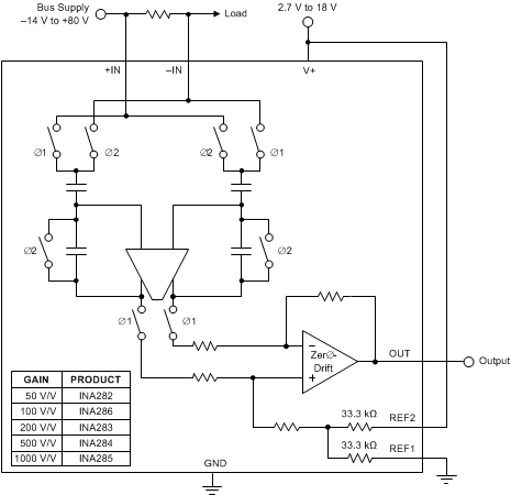
Detailed Block Diagram

INA282 INA283 INA284 INA285 INA286 fpd_bos485.gif