SBOS307G May 2004 – January 2015 INA193 , INA194 , INA195 , INA196 , INA197 , INA198
PRODUCTION DATA.
- 1 Features
- 2 Applications
- 3 Description
- 4 Revision History
- 5 Device Comparison Table
- 6 Pin Configuration and Functions
- 7 Specifications
- 8 Detailed Description
- 9 Application and Implementation
- 10Power Supply Recommendations
- 11Layout
- 12Device and Documentation Support
- 13Mechanical, Packaging, and Orderable Information
Package Options
Mechanical Data (Package|Pins)
- DBV|5
Thermal pad, mechanical data (Package|Pins)
Orderable Information
1 Features
- Wide Common-Mode Voltage:
−16 V to +80 V - Low Error: 3.0% Over Temp (maximum)
- Bandwidth: Up to 500 kHz
- Three Transfer Functions Available: 20 V/V, 50 V/V, and 100 V/V
- Quiescent Current: 900 μA (maximum)
- Complete Current Sense Solution
2 Applications
- Welding Equipment
- Notebook Computers
- Cell Phones
- Telecom Equipment
- Automotive
- Power Management
- Battery Chargers
3 Description
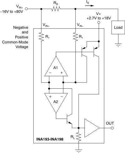
The INA193−INA198 family of current shunt monitors with voltage output can sense drops across shunts at common-mode voltages from −16 V to +80 V, independent of the INA19x supply voltage. They are available with three output voltage scales: 20 V/V, 50 V/V, and 100 V/V. The 500 kHz bandwidth simplifies use in current control loops. The INA193−INA195 devices provide identical functions but alternative pin configurations to the INA196−INA198 devices, respectively.
The INA193−INA198 devices operate from a single 2.7-V to 18-V supply, drawing a maximum of 900 μA of supply current. They are specified over the extended operating temperature range (−40°C to +125°C), and are offered in a space-saving SOT-23 package.
Device Information(1)
| PART NUMBER | PACKAGE | BODY SIZE (NOM) |
|---|---|---|
| INA193 | SOT-23 (5) | 2.90 mm × 1.60 mm |
| INA194 | ||
| INA195 | ||
| INA196 | ||
| INA197 | ||
| INA198 |
- For all available packages, see the orderable addendum at the end of the datasheet.
Simplified Schematic
