SBOS181F December 2000 – February 2017 INA139 , INA169
PRODUCTION DATA.
- 1 Features
- 2 Applications
- 3 Description
- 4 Revision History
- 5 Pin Configuration and Functions
- 6 Specifications
- 7 Detailed Description
-
8 Application and Implementation
- 8.1 Application Information
- 8.2 Typical Applications
- 9 Power Supply Recommendations
- 10Layout
- 11Device and Documentation Support
- 12Mechanical, Packaging, and Orderable Information
Package Options
Refer to the PDF data sheet for device specific package drawings
Mechanical Data (Package|Pins)
- DBV|5
Thermal pad, mechanical data (Package|Pins)
Orderable Information
1 Features
- Complete Unipolar High-Side Current Measurement Circuit
- Wide Supply and Common-Mode Range
- INA139: 2.7 V to 40 V
- INA169: 2.7 V to 60 V
- Independent Supply and Input Common-Mode Voltages
- Single Resistor Gain Set
- Low Quiescent Current: 60 µA (Typical)
- 5-Pin, SOT-23 Packages
2 Applications
- Current Shunt Measurement:
- Automotive, Telephone, Computers
- Portable and Battery-Backup Systems
- Battery Chargers
- Power Management
- Cell Phones
- Precision Current Source
3 Description
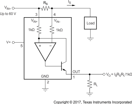
The INA139 and INA169 are high-side, unipolar, current shunt monitors. Wide input common-mode voltage range, high-speed, low quiescent current, and tiny SOT-23 packaging enable use in a variety of applications.
Input common-mode and power-supply voltages are independent and can range from 2.7 V to 40 V for the INA139 and 2.7 V to 60 V for the INA169. Quiescent current is only 60 µA, which permits connecting the power supply to either side of the current measurement shunt with minimal error.
The device converts a differential input voltage to a current output. This current is converted back to a voltage with an external load resistor that sets any gain from 1 to over 100. Although designed for current shunt measurement, the circuit invites creative applications in measurement and level shifting.
Both the INA139 and INA169 are available in 5-pin SOT-23 packages. The INA139 device is specified for the –40°C to +125°C temperature range, and the INA169 is specified from –40°C to +85°C.
Device Information(1)
| PART NUMBER | PACKAGE | BODY SIZE (NOM) |
|---|---|---|
| INA139 | SOT-23 (5) | 2.90 mm × 1.60 mm |
| INA169 |
- For all available packages, see the orderable addendum at the end of the data sheet.
