SLIS164E December 2014 – September 2016 DRV5033-Q1
PRODUCTION DATA.
- 1 Features
- 2 Applications
- 3 Description
- 4 Revision History
- 5 Pin Configuration and Functions
- 6 Specifications
- 7 Detailed Description
- 8 Application and Implementation
- 9 Power Supply Recommendations
- 10Layout
- 11Device and Documentation Support
- 12Mechanical, Packaging, and Orderable Information
Package Options
Mechanical Data (Package|Pins)
Thermal pad, mechanical data (Package|Pins)
Orderable Information
1 Features
- Digital Omnipolar-Switch Hall Sensor
- AEC-Q100 Qualified for Automotive Applications
- Grade 1: TA = –40 to 125°C (Q, See Device Nomenclature)
- Grade 0: TA = –40 to 150°C (E, See Device Nomenclature)
- Superior Temperature Stability
- BOP ±10% Over Temperature
- Multiple Sensitivity Options (BOP / BRP):
- ±3.5 / ±2 mT (FA, see Device Nomenclature)
- ±6.9 / ±3.5 mT (AJ, see Device Nomenclature)
- Detects North and South Magnetic Field
- Supports a Wide Voltage Range
- 2.7 to 38 V
- No External Regulator Required
- Open Drain Output (30-mA Sink)
- Fast 35-µs Power-On Time
- Small Package and Footprint
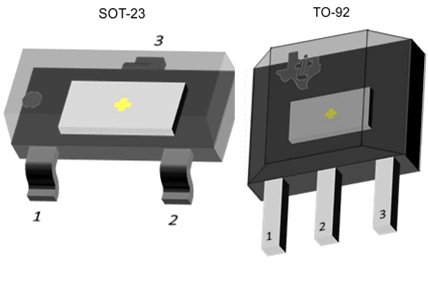
- Surface Mount 3-Pin SOT-23 (DBZ)
- 2.92 mm × 2.37 mm
- Through-Hole 3-Pin TO-92 (LPG)
- 4.00 mm × 3.15 mm
- Surface Mount 3-Pin SOT-23 (DBZ)
-
Protection Features
- Reverse Supply Protection (up to –22 V)
- Supports up to 40-V Load Dump
- Output Short-Circuit Protection
- Output Current Limitation
- OUT Short to Battery Protection
2 Applications
- Docking Detection
- Door Open and Close Detection
- Proximity Sensing
- Valve Positioning
- Pulse Counting
3 Description
The DRV5033-Q1 device is a chopper-stabilized Hall Effect Sensor that offers a magnetic sensing solution with superior sensitivity stability over temperature and integrated protection features.
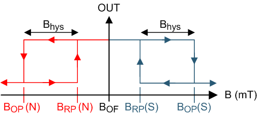
The DRV5033-Q1 responds the same to both polarities of magnetic field direction. When the applied magnetic flux density exceeds the BOP threshold, the DRV5033-Q1 open-drain output goes low. The output stays low until the field decreases to less than BRP, and then the output goes to high impedance. The output current sink capability is 30 mA. A wide operating voltage range from 2.7 to 38 V with reverse polarity protection up to –22 V makes the device suitable for a wide range of automotive applications.
Internal protection functions are provided for reverse supply conditions, load dump, and output short circuit or over current.
Device Information(1)
| PART NUMBER | PACKAGE | BODY SIZE (NOM) |
|---|---|---|
| DRV5033-Q1 | SOT-23 (3) | 2.92 mm × 1.30 mm |
| TO-92 (3) | 4.00 mm × 3.15 mm |
- For all available packages, see the orderable addendum at the end of the data sheet.
Output State

Device Packages
