SLVSCV1E September 2015 – February 2017 DRV3205-Q1
PRODUCTION DATA.
- 1 Features
- 2 Applications
- 3 Description
- 4 Revision History
- 5 Pin Configuration and Functions
- 6 Specifications
- 7 Detailed Description
- 8 Application and Implementation
- 9 Power Supply Recommendations
- 10Layout
- 11Device and Documentation Support
- 12Mechanical, Packaging, and Orderable Information
Package Options
Mechanical Data (Package|Pins)
- PHP|48
Thermal pad, mechanical data (Package|Pins)
- PHP|48
Orderable Information
1 Features
- AEC-Q100 Qualified for Automotive Applications:
- Device Temperature Grade 1: –40°C to +125°C Ambient Operating Temperature
- Three-Phase Bridge Driver for Motor Control
- Suitable for 12-V and 24-V Applications
- Three Integrated High-Accuracy Current Sense Amplifiers
- Integrated Boost Converter, Gate Drive to 4.75 V
- Drives 6 Separate N-Channel Power MOSFETs
- Strong 1-A Gate Drive for High-Current FETs
- Programmable Dead Time
- PWM Frequency up to 20 kHz
- Supports 100% Duty Cycle Operation
- Short-Circuit Protection
- VDS-Monitoring (Adjustable Detection Level)
- Shunt Current Limit (Adjustable Detection Level)
- Overvoltage and Undervoltage Protection
- Overtemperature Warning and Shut Down
- Sophisticated Failure Detection and Handling Through SPI
- System Supervision
- Q&A Watchdog
- I/O Supply Monitoring
- ADREF Monitoring
- Programmable Internal Fault Diagnostics
- Sleep Mode Function
- Thermally-Enhanced 48-Pin HTQFP PowerPAD™ IC Package (7-mm × 7-mm Body)
2 Applications
-
Automotive Motor-Control Applications
- Electrical Power Steering (EPS, EHPS)
- Electrical Brake and Brake Assist
- Transmission
- Pumps
- Industrial Motor-Control Applications
3 Description
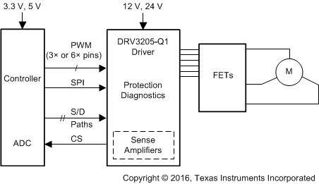
The DRV3205-Q1 bridge driver is dedicated to automotive three-phase brushless DC motor control applications. The device provides six dedicated drivers for standard-level N-channel MOSFET transistors. A boost converter with an integrated FET provides the overdrive voltage, allowing full control on the power stages even for low battery voltage down to 4.75 V. The strong driver strength is suitable for high-current applications and programmable to limit peak output current.
The device incorporates robust FET protection and system monitoring functions like a Q&A watchdog and voltage monitors for I/O supplies and ADC reference voltages. Integrated internal diagnostic functions can be accessed and programmed through an SPI interface.
Device Information(1)
| PART NUMBER | PACKAGE | BODY SIZE (NOM) |
|---|---|---|
| DRV3205-Q1 | HTQFP (48) | 7.00 mm × 7.00 mm |
- For all available packages, see the orderable addendum at the end of the data sheet.
Typical Application Diagram
