SLVSDP7A February 2017 – May 2017 DLPA1000
PRODUCTION DATA.
- 1 Features
- 2 Applications
- 3 Description
- 4 Revision History
- 5 Pin Configuration and Functions
- 6 Specifications
-
7 Detailed Description
- 7.1 Overview
- 7.2 Functional Block Diagram
- 7.3 Feature Description
- 7.4 Device Functional Modes
- 7.5 Programming
- 7.6
Register Maps
- 7.6.1 Chip ID (CHIPID) Register (address = 0x00h) [reset = A6h]
- 7.6.2 Enable (ENABLE) Register (address = 0x01h) [reset = 3h]
- 7.6.3 Switch Transient Current Limit (IREG) Register (address = 0x02h) [reset = 28h]
- 7.6.4 SW4 LED DC Regulation Current, MSB (SW4MSB) Register (address = 0x03h) [reset = 0h]
- 7.6.5 SW4 LED DC Regulation Current, LSB (SW4LSB) Register (address = 0x04h) [reset = 0h]
- 7.6.6 SW5 LED DC Regulation Current, MSB (SW5MSB) Register (address = 0x05h) [reset = 0h]
- 7.6.7 SW5 LED DC Regulation Current, LSB (SW5LSB) Register (address = 0x06h) [reset = 0h]
- 7.6.8 SW6 LED DC Regulation Current, MSB (SW6MSB) Register (address = 0x07h) [reset = 0h]
- 7.6.9 SW6 LED DC Regulation Current, LSB (SW6LSB) Register (address = 0x08h) [reset = 0h]
- 7.6.10 Analog Front End Control (AFE) Register (address = 0x0Ah) [reset = 0h]
- 7.6.11 Strobe Decode - Break Before Make Timing Control (BBM) Register (address = 0x0Bh) [reset = 0h]
- 7.6.12 Interrupt (INT) Register (address = 0x0Ch) [reset = X]
- 7.6.13 Interrupt Mask (MASK) Register (address = 0x0Dh) [reset = 0h]
- 7.6.14 Password (PASSWORD) Register (address = 0x10h) [reset = 0h]
- 7.6.15 System Configuration (SYSTEM) Register (address = 0x11h) [reset = 0h]
- 7.6.16 EEPROM User Register, Byte0 (BYTE0) (address = 0x20h) [reset = 0h]
- 7.6.17 EEPROM User Register, Byte1 (BYTE1) (address = 0x21h) [reset = 0h]
- 7.6.18 EEPROM User Register, Byte2 (BYTE2) (address = 0x22h) [reset = 0h]
- 7.6.19 EEPROM User Register, Byte3 (BYTE3) (address = 0x23h) [reset = 0h]
- 7.6.20 EEPROM User Register, Byte4 (BYTE4) (address = 0x24h) [reset = 0h]
- 7.6.21 EEPROM User Register, Byte5 (BYTE5) (address = 0x25h) [reset = 0h]
- 7.6.22 EEPROM User Register, Byte6 (BYTE6) (address = 0x26h) [reset = 0h]
- 7.6.23 EEPROM User Register, Byte7 (BYTE7) (address = 0x27h) [reset = 0h]
- 8 Application and Implementation
- 9 Power Supply Recommendations
- 10Layout
- 11Device and Documentation Support
- 12Mechanical, Packaging, and Orderable Information
Package Options
Refer to the PDF data sheet for device specific package drawings
Mechanical Data (Package|Pins)
- YFF|49
Thermal pad, mechanical data (Package|Pins)
Orderable Information
1 Features
- High-Efficiency RGB LED Driver With Buck-Boost DC-to-DC Converter and Integrated MOSFETS
- Six Low-Impedance (<100 mΩ) MOSFET Switches for Channel Selection
- Independent, 10-Bit Current Control per Channel
- DMD Regulators
- Requires Only a Single Inductor
- VOFS: 8.5 V
- VBIAS: 16 V
- VRST: –10 V
- Reset Generation and Power Supply Sequencing
- RGB LED Strobe Decoder Supports:
- Common-Anode RGBs
- Cathode-Cathode-Anode RGBs
- 33-MHz Serial Peripheral Interface (SPI)
- Multiplexer for Measuring Analog Signals
- Battery Voltage
- LED Voltage, LED Current
- Light Sensor (for White Point Correction)
- External Temperature Sensor
- Monitoring and Protection Circuits
- Hot Die Warning and Thermal Shutdown
- Low-Battery and Undervoltage Lockout
- Overcurrent and Undervoltage Protection
- 49-Ball 0.4-mm Pitch, DSBGA Package
2 Applications
3 Description
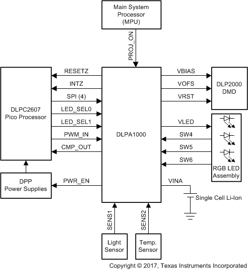
DLPA1000 is a dedicated PMIC / RGB LED driver for the DLP2000 Digital Micromirror Devices (DMD) when used with a DLPC2607 digital controller. For reliable operation of these chipsets, it is mandatory to use the DLPA1000.
Device Information(1)
| PART NUMBER | PACKAGE | BODY SIZE (NOM) |
|---|---|---|
| DLPA1000 | DSBGA (49) | 2.40 mm × 2.40 mm |
- For all available packages, see the orderable addendum at the end of the data sheet.
Simplified Schematic
