SBAS349F August 2005 – June 2016 DAC8812
PRODUCTION DATA.
- 1 Features
- 2 Applications
- 3 Description
- 4 Revision History
- 5 Device Comparison Table
- 6 Pin Configuration and Functions
- 7 Specifications
- 8 Detailed Description
- 9 Application and Implementation
- 10Power Supply Recommendations
- 11Layout
- 12Device and Documentation Support
- 13Mechanical, Packaging, and Orderable Information
Package Options
Mechanical Data (Package|Pins)
- PW|16
Thermal pad, mechanical data (Package|Pins)
Orderable Information
1 Features
- Relative Accuracy: 1 LSB Max
- Differential Nonlinearity: 1 LSB Max
- 2-mA Full-Scale Current ±20%,
With VREF = ±10 V - 0.5-μs Settling Time
- Midscale or Zero-Scale Reset
- Separate 4Q Multiplying Reference Inputs
- Reference Bandwidth: 10 MHz
- Reference Dynamics: –105-dB THD
- SPI™-Compatible 3-Wire Interface:
50 MHz -
Double Buffered Registers to Enable
Simultaneous Multichannel Update - Internal Power-On Reset
- Industry-Standard Pin Configuration
2 Applications
- Automatic Test Equipment
- Instrumentation
- Digitally Controlled Calibration
3 Description
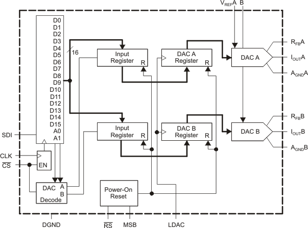
The DAC8812 is a dual, 16-bit, current-output digital-to-analog converter (DAC) designed to operate from a single 2.7-V to 5.5-V supply.
The applied external reference input voltage VREF determines the full-scale output current. An internal feedback resistor (RFB) provides temperature tracking for the full-scale output when combined with an external I-to-V precision amplifier.
A double-buffered, serial data interface offers high-speed, 3-wire, SPI and microcontroller compatible inputs using serial data in (SDI), clock (CLK), and a chip-select (CS). A common level-sensitive load DAC strobe (LDAC) input allows simultaneous update of all DAC outputs from previously loaded input registers. Additionally, an internal power-on reset forces the output voltage to zero at system turnon. An MSB pin allows system reset assertion (RS) to force all registers to zero code when MSB = 0, or to midscale code when MSB = 1.
Device Information(1)
| PART NUMBER | PACKAGE | BODY SIZE (NOM) |
|---|---|---|
| DAC8812 | TSSOP (16) | 5.00 mm × 4.40 mm |
Space
Space
