SLVSBY7 February 2017 DAC8775
PRODUCTION DATA.
- 1 Features
- 2 Applications
- 3 Description
- 4 Revision History
- 5 Device Comparison Table
- 6 Pin Configuration and Functions
- 7 Specifications
-
8 Detailed Description
- 8.1 Overview
- 8.2 Functional Block Diagram
- 8.3
Feature Description
- 8.3.1 Current Output Stage
- 8.3.2 Voltage Output Stage
- 8.3.3 Buck-Boost Converter
- 8.3.4 Analog Power Supply
- 8.3.5 Digital Power Supply
- 8.3.6 Internal Reference
- 8.3.7 Power-On-Reset
- 8.3.8 ALARM Pin
- 8.3.9 Power GOOD Bits
- 8.3.10 Status Register
- 8.3.11 Status Mask
- 8.3.12 Alarm Action
- 8.3.13 Watchdog Timer
- 8.3.14 Programmable Slew Rate
- 8.3.15 HART Interface
- 8.4 Device Functional Modes
- 8.5
Register Maps
- 8.5.1 DAC8775 Commands
- 8.5.2
Register Maps and Bit Functions
- 8.5.2.1 No Operation Register (address = 0x00) [reset = 0x0000]
- 8.5.2.2 Reset Register (address = 0x01) [reset = 0x0000]
- 8.5.2.3 Reset Config Register (address = 0x02) [reset = 0x0000]
- 8.5.2.4 Select DAC Register (address = 0x03) [reset = 0x0000]
- 8.5.2.5 Configuration DAC Register (address = 0x04) [reset = 0x0000]
- 8.5.2.6 DAC Data Register (address = 0x05) [reset = 0x0000]
- 8.5.2.7 Select Buck-Boost Converter Register (address = 0x06) [reset = 0x0000]
- 8.5.2.8 Configuration Buck-Boost Register (address = 0x07) [reset = 0x0000]
- 8.5.2.9 DAC Channel Calibration Enable Register (address = 0x08) [reset = 0x0000]
- 8.5.2.10 DAC Channel Gain Calibration Register (address = 0x09) [reset = 0x0000]
- 8.5.2.11 DAC Channel Offset Calibration Register (address = 0x0A) [reset = 0x0000]
- 8.5.2.12 Status Register (address = 0x0B) [reset = 0x1000]
- 8.5.2.13 Status Mask Register (address = 0x0C) [reset = 0x0000]
- 8.5.2.14 Alarm Action Register (address = 0x0D) [reset = 0x0000]
- 8.5.2.15 User Alarm Code Register (address = 0x0E) [reset = 0x0000]
- 8.5.2.16 Reserved Register (address = 0x0F) [reset = N/A]
- 8.5.2.17 Write Watchdog Timer Register (address = 0x10) [reset = 0x0000]
- 8.5.2.18 Device ID Register (address = 0x11) [reset = 0x0000]
- 8.5.2.19 Reserved Register (address 0x12 - 0xFF) [reset = N/A]
- 9 Application and Implementation
- 10Power Supply Recommendations
- 11Layout
- 12Device and Documentation Support
- 13Mechanical, Packaging, and Orderable Information
Package Options
Mechanical Data (Package|Pins)
- RWF|72
Thermal pad, mechanical data (Package|Pins)
Orderable Information
1 Features
- Output Current:
- 0 mA to 24 mA; 3.5 mA to 23.5 mA; 0 mA to 20 mA; 4 mA to 20 mA; ±24 mA
- Output Voltage (with/without 20% over-range):
- 0 V to 5 V; 0 V to 10 V; ±5 V; ±10 V
- 0 V to 6 V; 0 V to 12 V; ±6 V; ±12 V
- Adaptive Power Management
- Single Wide Power Supply Pin (12 V – 36 V )
- ±0.1% FSR Total Unadjusted Error (TUE)
- DNL: ±1 LSB Max
- Internal 5-V Reference (10 ppm/°C max)
- Internal 5-V Digital Power Supply Output
- CRC/Frame Error Check, Watchdog Timer
- Thermal Alarm, Open/Short Circuit for System Reliability
- Safe Actions on Alarm Condition
- Auto Learn Load Detection
- Wide Temperature Range: –40°C to +125°C
2 Applications
- 4-mA to 20-mA Current Loops
- Analog Output Modules
- Programmable Logic Controllers (PLCs)
- Building Automation
- Sensor Transmitters
- Process Control
3 Description
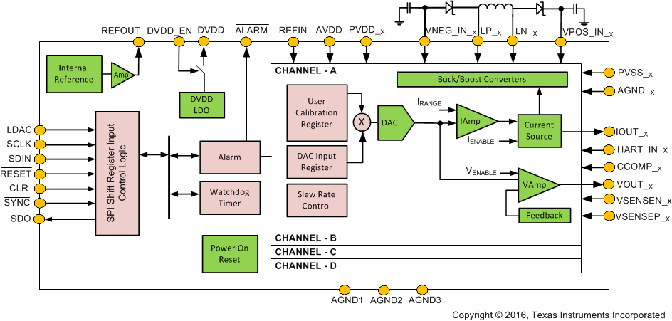
The DAC8775 is a quad-channel precision, fully integrated, 16-bit, digital-to-analog converter (DAC) with adaptive power management, and is designed to meet the requirements of industrial control applications. The adaptive power management circuit, when enabled, minimizes the power dissipation of the chip. When programmed as a current output, the supply voltage on the current output driver is regulated between 4.5 V and 32 V based on continuous feedback of voltage on the current output pin via an integrated buck/boost converter. When programmed as a voltage output, this circuit generates a programmable supply voltage for the voltage output stage (±15 V). DAC8775 also contains an LDO to generate the digital supply (5 V) from a single power supply pin.
DAC8775 is also implemented with a Highway Addressable Remote Transducer (HART) Signal Interface to superimpose an external HART signal on the current output. The slew rate of the current output DAC is register programmable. The device can operate with a single external power supply of +12 V to +36 V using the integrated buck/boost converters or with external power supplies when the buck/boost converters are disabled.
Device Information(1)
| PART NUMBER | PACKAGE | BODY SIZE (NOM) |
|---|---|---|
| DAC8775 | VQFN (72) | 10.00 mm x 10.00 mm |
- For all available packages, see the orderable addendum at the end of the data sheet.
Block Diagram
