SLPS264D October 2010 – May 2015 CSD86330Q3D
PRODUCTION DATA.
- 1Features
- 2Applications
- 3Description
- 4Revision History
- 5Specifications
- 6Application and Implementation
- 7Recommended PCB Design Overview
- 8Device and Documentation Support
- 9Mechanical, Packaging, and Orderable Information
Package Options
Refer to the PDF data sheet for device specific package drawings
Mechanical Data (Package|Pins)
- DQZ|8
Thermal pad, mechanical data (Package|Pins)
Orderable Information
1 Features
- Half-Bridge Power Block
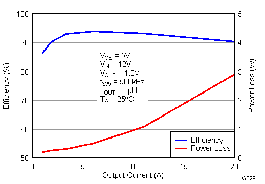
- 90% System Efficiency at 15 A
- Up to 20 A Operation
- High Frequency Operation (Up To 1.5 MHz)
- High Density – SON 3.3 mm × 3.3 mm Footprint
- Optimized for 5 V Gate Drive
- Low Switching Losses
- Ultra Low Inductance Package
- RoHS Compliant
- Halogen Free
- Pb-Free Terminal Plating
2 Applications
- Synchronous Buck Converters
- High Frequency Applications
- High Current, Low Duty Cycle Applications
- Multiphase Synchronous Buck Converters
- POL DC-DC Converters
- IMVP, VRM, and VRD Applications
3 Description
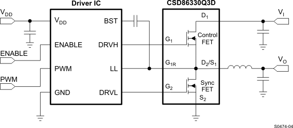
The CSD86330Q3D NexFET™ power block is an optimized design for synchronous buck applications offering high current, high efficiency, and high frequency capability in a small 3.3 mm × 3.3 mm outline. Optimized for 5 V gate drive applications, this product offers a flexible solution capable of offering a high density power supply when paired with any 5 V gate drive from an external controller/driver.
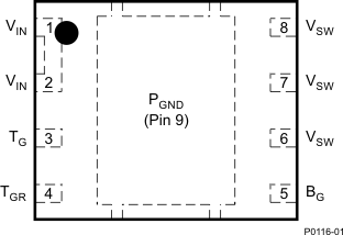
Top View

Ordering Information(1)
| Device | Media | Qty | Package | Ship |
|---|---|---|---|---|
| CSD86330Q3D | 13-Inch Reel | 2500 | SON 3.3 mm × 3.3 mm Plastic Package | Tape and Reel |
| CSD86330Q3DT | 7-Inch Reel | 250 |
- For all available packages, see the orderable addendum at the end of the data sheet.
RDS(on) vs VGS |
Gate Charge |