SLPS454B December 2013 – January 2016 CSD25402Q3A
PRODUCTION DATA.
- 1Features
- 2Applications
- 3Description
- 4Revision History
- 5Specifications
- 6Device and Documentation Support
- 7Mechanical, Packaging, and Orderable Information
Package Options
Mechanical Data (Package|Pins)
- DNH|8
Thermal pad, mechanical data (Package|Pins)
Orderable Information
1 Features
- Ultra-Low Qg and Qgd
- Low Thermal Resistance
- Low RDS(on)
- Pb and Halogen Free
- RoHS Compliant
- SON 3.3 mm × 3.3 mm Plastic Package
2 Applications
- DC-DC Converters
- Battery Management
- Load Switch
- Battery Protection
3 Description
This –20-V, 7.7-mΩ NexFET™ power MOSFET is designed to minimize losses in power conversion load management applications with a SON 3.3 mm × 3.3 mm package that offers an excellent thermal performance for the size of the device.
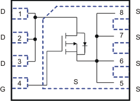
Top View

Product Summary
| TA = 25°C | TYPICAL VALUE | UNIT | ||
|---|---|---|---|---|
| VDS | Drain-to-source voltage | –20 | V | |
| Qg | Gate charge total (–4.5 V) | 7.5 | nC | |
| Qgd | Gate charge gate to drain | 1.1 | nC | |
| RDS(on) | Drain-to-source on resistance | VGS = –1.8 V | 74 | mΩ |
| VGS = –2.5 V | 13.3 | mΩ | ||
| VGS = –4.5 V | 7.7 | mΩ | ||
| Vth | Threshold voltage | –0.9 | V | |
Ordering Information(1)
| DEVICE | QTY | MEDIA | PACKAGE | SHIP |
|---|---|---|---|---|
| CSD25402Q3A | 2500 | 13-Inch Reel | SON 3.3 mm × 3.3 mm Plastic Package | Tape and Reel |
| CSD25402Q3AT | 250 | 7-Inch Reel |
- For all available packages, see the orderable addendum at the end of the data sheet.
Absolute Maximum Ratings
| TA = 25°C | VALUE | UNIT | |
|---|---|---|---|
| VDS | Drain-to-source voltage | –20 | V |
| VGS | Gate-to-source voltage | +12 or –12 | V |
| ID | Continuous drain current, TC = 25°C | –76 | A |
| Continuous drain current (package limit) | –35 | A | |
| Continuous drain current(1) | –15 | A | |
| IDM | Pulsed drain current(2) | –148 | A |
| PD | Power dissipation(1) | 2.8 | W |
| Power dissipation, TC = 25°C | 69 | ||
| TJ | Operating junction temperature | –55 to 150 | °C |
| Tstg | Storage temperature | –55 to 150 | °C |
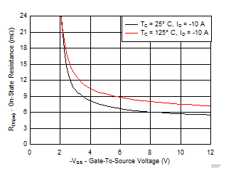
RDS(on) vs VGS |
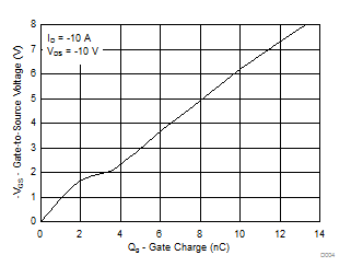
Gate Charge |