SBAS543C August 2011 – February 2016 ADS8528 , ADS8548 , ADS8568
PRODUCTION DATA.
- 1 Features
- 2 Applications
- 3 Description
- 4 Revision History
- 5 Device Comparison Table
- 6 Pin Configuration and Functions
-
7 Specifications
- 7.1 Absolute Maximum Ratings
- 7.2 ESD Ratings
- 7.3 Recommended Operating Conditions
- 7.4 Thermal Information
- 7.5 Electrical Characteristics: General
- 7.6 Electrical Characteristics: ADS8528
- 7.7 Electrical Characteristics: ADS8548
- 7.8 Electrical Characteristics: ADS8568
- 7.9 Serial Interface Timing Requirements
- 7.10 Parallel Interface Timing Requirements (Read Access)
- 7.11 Parallel Interface Timing Requirements (Write Access)
- 7.12 Typical Characteristics
- 8 Parameter Measurement information
- 9 Detailed Description
- 10Application and Implementation
- 11Power Supply Recommendations
- 12Layout
- 13Device and Documentation Support
- 14Mechanical, Packaging, and Orderable Information
Package Options
Mechanical Data (Package|Pins)
Thermal pad, mechanical data (Package|Pins)
- RGC|64
Orderable Information
1 Features
- Family of 12-, 14-, and 16-Bit, Pin- and Software-Compatible ADCs
- Maximum Data Rate per Channel:
- ADS8528: 650 kSPS (PAR) or
480 kSPS (SER) - ADS8548: 600 kSPS (PAR) or
450 kSPS (SER) - ADS8568: 510 kSPS (PAR) or
400 kSPS (SER)
- ADS8528: 650 kSPS (PAR) or
- Excellent AC Performance:
- Signal-to-Noise Ratio:
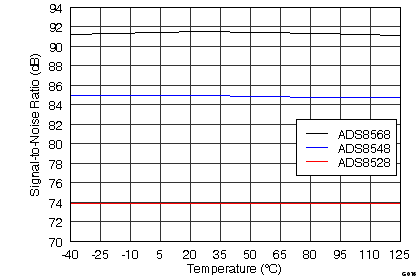
ADS8528: 73.9 dB, ADS8548: 85 dB, ADS8568: 91.5 dB - Total Harmonic Distortion:
ADS8528: –89 dB, ADS8548: –91 dB, ADS8568: –94 dB
- Signal-to-Noise Ratio:
- Programmable, Buffered Internal Reference:
0.5 V–2.5 V or 0.5 V–3.0 V Supports Input Voltage Ranges up to ±12 V - Selectable Parallel or Serial Interface
- Scalable Low-Power Operation Using Auto-Sleep Mode: Only 32 mW at 10 kSPS
- Fully Specified Over Extended Industrial Temperature Range
2 Applications
- Protection Relays
- Power Quality Measurement
- Multi-Axis Motor Controls
- Programmable Logic Controllers
- Industrial Data Acquisition
SNR vs Temperature

3 Description
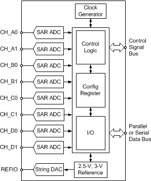
The ADS85x8 contain eight low-power, 12-, 14-, or 16-bit, successive approximation register (SAR)-based analog-to-digital converters (ADCs) with true bipolar inputs. These channels are grouped in four pairs, thus allowing simultaneous high-speed signal acquisition of up to 650 kSPS.
The devices support selectable parallel or serial interface with daisy-chain capability. The programmable reference allows handling of analog input signals with amplitudes up to ±12 V.
The ADS85x8 family supports an auto-sleep mode for minimum power dissipation and is available in both 64-pin VQFN and LQFP packages. The entire family is specified over a temperature range of –40°C to +125°C.
Device Information(1)
| PART NUMBER | PACKAGE | BODY SIZE (NOM) |
|---|---|---|
| ADS85x8 | VQFN (64) | 9.00 mm × 9.00 mm |
| LQFP (64) | 10.00 mm × 10.00 mm |
- For all available packages, see the orderable addendum at the end of the data sheet.
Simplified Block Diagram

4 Revision History
Changes from B Revision (November 2015) to C Revision
Changes from A Revision (October 2011) to B Revision
- Added ESD Ratings table, Recommended Operating Conditions table, Feature Description section, Device Functional Modes section, Register Maps section, Application and Implementation section, Power Supply Recommendations section, Layout section, Device and Documentation Support section, and Mechanical, Packaging, and Orderable Information sectionGo
- Changed title of Device Comparison Table, deleted footnote 1 Go
- Added Storage temperature parameter to Absolute Maximum Ratings tableGo
- Changed Clock cycles per conversion to be a single parameter instead of part of tCONV parameter in Serial Interface Timing Requirements table Go
- Changed tBUFS parameter in Serial Interface Timing Requirements tableGo
- Added footnote 3 to Serial Interface Timing Requirements tableGo
- Changed Clock cycles per conversion to be a single parameter instead of part of tCONV parameter in Parallel Interface Timing Requirements (Read Access) table Go
- Changed tBUCS parameter in Parallel Interface Timing Requirements (Read Access) table Go
- Added footnote 3 to Parallel Interface Timing Requirements (Read Access) table Go
- Changed Data Readout and BUSY/INT Signal sectionGo
- Added Sequential Operation sectionGo
- Changed description of initiating a new conversion in Reset and Power-Down Modes sectionGo
Changes from * Revision (August 2011) to A Revision