SBASA31B November   2020  – November 2021 ADS131B04-Q1

PRODUCTION DATA  

  1. Features
  2. Applications
  3. Description
  4. Revision History
  5. Pin Configuration and Functions
  6. Specifications
    1. 6.1 Absolute Maximum Ratings
    2. 6.2 ESD Ratings
    3. 6.3 Recommended Operating Conditions
    4. 6.4 Thermal Information
    5. 6.5 Electrical Characteristics
    6. 6.6 Timing Requirements
    7. 6.7 Switching Characteristics
    8. 6.8 Timing Diagrams
    9. 6.9 Typical Characteristics
  7. Parameter Measurement Information
    1. 7.1 Noise Measurements
  8. Detailed Description
    1. 8.1 Overview
    2. 8.2 Functional Block Diagram
    3. 8.3 Feature Description
      1. 8.3.1  Input ESD Protection Circuitry
      2. 8.3.2  Input Multiplexer
      3. 8.3.3  Programmable Gain Amplifier (PGA)
      4. 8.3.4  Voltage Reference
      5. 8.3.5  Internal Test Signals
      6. 8.3.6  Clocking
        1. 8.3.6.1 External Clock Using CLKIN Pin
        2. 8.3.6.2 Internal Oscillator
      7. 8.3.7  ΔΣ Modulator
      8. 8.3.8  Digital Filter
        1. 8.3.8.1 Digital Filter Implementation
          1. 8.3.8.1.1 Fast-Settling Filter
          2. 8.3.8.1.2 SINC3 and SINC3 + SINC1 Filter
        2. 8.3.8.2 Digital Filter Characteristic
      9. 8.3.9  Calibration Registers
      10. 8.3.10 Register Map CRC
    4. 8.4 Device Functional Modes
      1. 8.4.1 Power-Up and Reset
        1. 8.4.1.1 Power-On Reset
        2. 8.4.1.2 SYNC/RESET Pin
        3. 8.4.1.3 RESET Command
      2. 8.4.2 Fast Start-Up Behavior
      3. 8.4.3 Conversion Modes
        1. 8.4.3.1 Continuous-Conversion Mode
        2. 8.4.3.2 Global-Chop Mode
      4. 8.4.4 Power Modes
      5. 8.4.5 Standby Mode
      6. 8.4.6 Synchronization
    5. 8.5 Programming
      1. 8.5.1 Serial Interface
        1. 8.5.1.1  Chip Select (CS)
        2. 8.5.1.2  Serial Data Clock (SCLK)
        3. 8.5.1.3  Serial Data Input (DIN)
        4. 8.5.1.4  Serial Data Output (DOUT)
        5. 8.5.1.5  Data Ready (DRDY)
        6. 8.5.1.6  SPI Communication Frames
        7. 8.5.1.7  SPI Communication Words
        8. 8.5.1.8  Short SPI Frames
        9. 8.5.1.9  Communication Cyclic Redundancy Check (CRC)
        10. 8.5.1.10 SPI Timeout
      2. 8.5.2 ADC Conversion Data Format
      3. 8.5.3 Commands
        1. 8.5.3.1 NULL (0000 0000 0000 0000)
        2. 8.5.3.2 RESET (0000 0000 0001 0001)
        3. 8.5.3.3 STANDBY (0000 0000 0010 0010)
        4. 8.5.3.4 WAKEUP (0000 0000 0011 0011)
        5. 8.5.3.5 LOCK (0000 0101 0101 0101)
        6. 8.5.3.6 UNLOCK (0000 0110 0110 0110)
        7. 8.5.3.7 RREG (101a aaaa annn nnnn)
          1. 8.5.3.7.1 Reading a Single Register
          2. 8.5.3.7.2 Reading Multiple Registers
        8. 8.5.3.8 WREG (011a aaaa annn nnnn)
      4. 8.5.4 Collecting Data for the First Time or After a Pause in Data Collection
    6. 8.6 Register Map
  9. Application and Implementation
    1. 9.1 Application Information
      1. 9.1.1 Troubleshooting
      2. 9.1.2 Unused Inputs and Outputs
      3. 9.1.3 Antialias Filter
      4. 9.1.4 Minimum Interface Connections
      5. 9.1.5 Multiple Device Configuration
    2. 9.2 Typical Application
      1. 9.2.1 Design Requirements
      2. 9.2.2 Detailed Design Procedure
        1. 9.2.2.1 Current Shunt Measurement
        2. 9.2.2.2 Battery Pack Voltage Measurement
        3. 9.2.2.3 Shunt Temperature Measurement
        4. 9.2.2.4 Auxiliary Analog Supply Voltage Measurement
      3. 9.2.3 Application Curves
  10. 10Power Supply Recommendations
    1. 10.1 CAP Pin Capacitor Requirement
    2. 10.2 Power-Supply Sequencing
    3. 10.3 Power-Supply Decoupling
  11. 11Layout
    1. 11.1 Layout Guidelines
    2. 11.2 Layout Example
  12. 12Device and Documentation Support
    1. 12.1 Documentation Support
      1. 12.1.1 Related Documentation
    2. 12.2 Receiving Notification of Documentation Updates
    3. 12.3 Support Resources
    4. 12.4 Trademarks
    5. 12.5 Electrostatic Discharge Caution
    6. 12.6 Glossary
  13. 13Mechanical, Packaging, and Orderable Information

Package Options

Mechanical Data (Package|Pins)
Thermal pad, mechanical data (Package|Pins)
Orderable Information

Features

  • AEC-Q100 qualified for automotive applications:
    • Temperature grade 1: –40°C to +125°C, TA
  • Functional Safety-Capable
  • 4 simultaneous-sampling, differential input ADCs
  • Programmable data rate: Up to 32 kSPS
  • Programmable gain: Up to 128
  • Noise performance:
    • 0.82 μVRMS at 1 kSPS, gain = 8
  • Global-chop mode to remove offset drift over temperature and time
  • High-impedance analog inputs for direct sensor connection
  • Integrated negative charge pump allows input signal measurements below ground
  • Crosstalk between channels: –120 dB
  • Low-drift internal reference: 1.2 V
  • Precision internal oscillator
  • CRC on communications and register map
  • Analog and digital supplies: 2.7 V to 3.6 V
  • Low power consumption: 5 mW at 3.3-V AVDD and DVDD
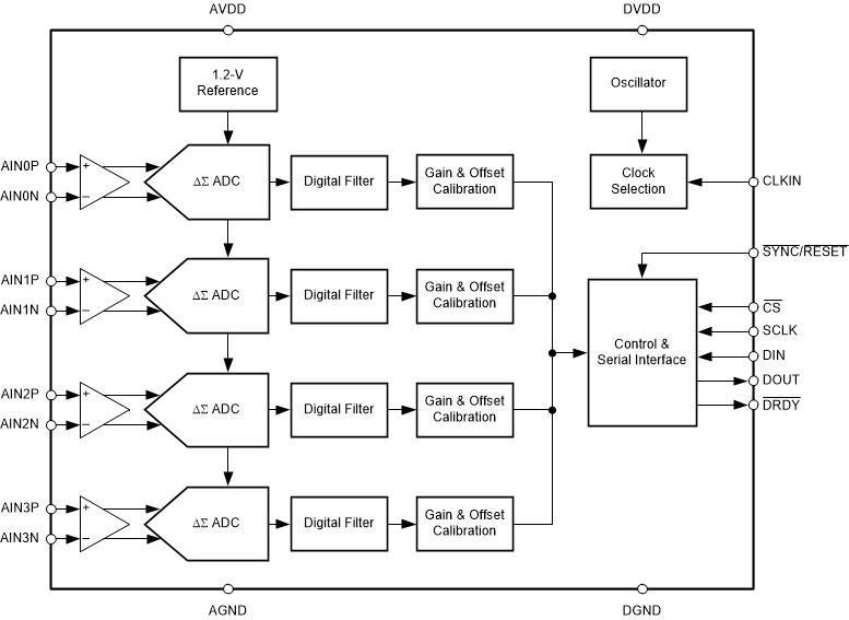
GUID-20210123-CA0I-327F-2FVK-VPZBHKSZNVZP-low.gif Simplified Block Diagram