SNAS411P August 2008 – April 2017 ADC128S102QML-SP
PRODUCTION DATA.
- 1 Features
- 2 Applications
- 3 Description
- 4 Revision History
- 5 Pin Configuration and Functions
-
6 Specifications
- 6.1 Absolute Maximum Ratings
- 6.2 ESD Ratings
- 6.3 Recommended Operating Conditions
- 6.4 Thermal Information
- 6.5 Electrical Characteristics: ADC128S102QML-SP Converter
- 6.6 Electrical Characteristics: Radiation
- 6.7 Electrical Characteristics: Burn in Delta Parameters - TA at 25°C
- 6.8 Timing Requirements
- 6.9 Typical Characteristics
- 7 Detailed Description
- 8 Application and Implementation
- 9 Power Supply Recommendations
- 10Layout
- 11Device and Documentation Support
- 12Mechanical, Packaging, and Orderable Information
Package Options
Refer to the PDF data sheet for device specific package drawings
Mechanical Data (Package|Pins)
- NAC|16
- Y|0
- NAD|16
Thermal pad, mechanical data (Package|Pins)
Orderable Information
1 Features
-
5962R07227
- Total Ionizing Dose 100 krad(Si)
- Single Event Latch-Up Immune 120 MeV-cm2/mg
- Single Event Functional Interrupt Immune 120 MeV-cm2/mg
(See Radiation Report)
- Eight Input Channels
- Variable Power Management
- Independent Analog and Digital Supplies
- SPI™/QSPI™/MICROWIRE™/DSP Compatible
- Packaged in 16-Lead Ceramic SOIC
- Key Specifications
- Conversion Rate: 50 kSPS to 1 MSPS
- DNL (VA = VD = 5 V): +1.5 / −0.9 LSB (Maximum)
- INL (VA = VD = 5 V): +1.4 / −1.25 LSB (Maximum)
- Power Consumption
- 3-V Supply: 2.3 mW (Typical)
- 5-V Supply: 10.7 mW (Typical)
2 Applications
- Satellites
- Attitude and Orbit Control
- Precision Sensors
- Motor Control
- High Temperature
- Medical Systems
- Accelerators
3 Description
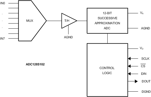
The ADC128S102 device is a low-power, eight-channel CMOS 12-bit analog-to-digital converter specified for conversion throughput rates of 50 kSPS to 1 MSPS. The converter is based on a successive-approximation register architecture with an internal track-and-hold circuit. The device can be configured to accept up to eight input signals at inputs IN0 through IN7.
The output serial data is straight binary and is compatible with several standards, such as SPI, QSPI, MICROWIRE, and many common DSP serial interfaces.
The ADC128S102 may be operated with independent analog and digital supplies. The analog supply (VA) can range from 2.7 V to 5.25 V, and the digital supply (VD) can range from 2.7 V to VA. Normal power consumption using a 3-V or 5-V supply is 2.3 mW and 10.7 mW, respectively. The power-down feature reduces the power consumption to 0.06 µW using a 3-V supply and 0.25 µW using a 5-V supply.
Device Information(1)
- For all available packages, see the orderable addendum at the end of the data sheet.
Block Diagram
