SLLSF07 September 2017 TUSB215-Q1
PRODUCTION DATA.
- 1 Features
- 2 Applications
- 3 Description
- 4 Revision History
- 5 Pin Configuration and Functions
- 6 Specifications
- 7 Detailed Description
- 8 Application and Implementation
- 9 Power Supply Recommendations
- 10Layout
- 11Device and Documentation Support
- 12Mechanical, Packaging, and Orderable Information
Package Options
Refer to the PDF data sheet for device specific package drawings
Mechanical Data (Package|Pins)
- RGY|14
Thermal pad, mechanical data (Package|Pins)
Orderable Information
1 Features
- Qualified for Automotive Applications
- AEC-Q100 Qualified with the Following Results
- Device Temperature Grade 2: –40°C to 105°C Ambient Operating Temperature
- Device HBM Classification Level H1C
- Device CDM Classification Level C3
- Compatible with USB 2.0, OTG 2.0 and BC 1.2
- Pin strap or I2C Configurable
- USB BC1.2 Charging Downstream Port (CDP) controller
- Support for LS, FS, HS signaling
- Ultra-low USB Disconnect and Shutdown Power Consumption
- Scalable solution - Daisy Chain Device for High Loss Applications
- D1P/M and D2P/M Interchangeable and Host/Device Agnostic
- Supports up to 5m pre-channel or 2m post-channel Cable Length
- Four Selectable AC Boost Setting Via External Pulldown Resistor
- DC Boost Along With AC Boost for Best Signal Integrity
2 Applications
- Automotive Infotainment
- Notebooks
- Desktops
- Docking Stations
- Tablets
- Cell Phones
- Active Cable, Cable Extenders
- Backplane
- Televisions
3 Description
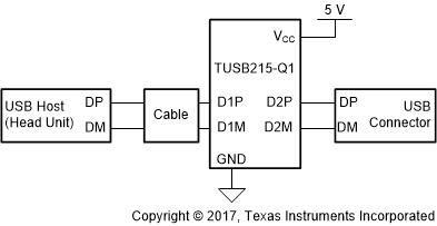
The TUSB215-Q1 is a USB High-Speed (HS) signal conditioner, designed to compensate for ISI signal loss in a transmission channel which helps passing USB electrical compliance tests.
TUSB215-Q1 has a patent-pending design which is agnostic to USB Low Speed (LS) and Full Speed (FS) signals. LS and FS signal characteristics are unaffected by the TUSB215-Q1 while HS signals are compensated.
Programmable signal AC boost and DC boost permits fine tuning device performance to optimize High Speed signals at the connector, this allows use in many different applications.
In addition, TUSB215-Q1 is compatible with the USB On-The-Go (OTG) and Battery Charging (BC) protocols. TUSB215-Q1 further acts as Charging Downstream Port (CDP) controller and handles the necessary handshakes with the downstream device.
Device Information (1)
| PART NUMBER | PACKAGE | BODY SIZE (NOM) |
|---|---|---|
| TUSB215-Q1 | VQFN (14) | 3.50 mm x 3.50 mm |
- For all available packages, see the orderable addendum at the end of the datasheet.
SPACER
Simplified Schematic

Display
