SLVS351P September 2002 – March 2015
PRODUCTION DATA.
- 1 Features
- 2 Applications
- 3 Description
- 4 Revision History
- 5 Pin Configuration and Functions
- 6 Specifications
- 7 Detailed Description
- 8 Application and Implementation
- 9 Power Supply Recommendations
- 10Layout
- 11Device and Documentation Support
- 12Mechanical, Packaging, and Orderable Information
Package Options
Mechanical Data (Package|Pins)
Thermal pad, mechanical data (Package|Pins)
Orderable Information
1 Features
- 1-A Low-Dropout Regulator With Enable
- Available in Fixed and Adjustable (1.2 V to 5.5 V) Versions
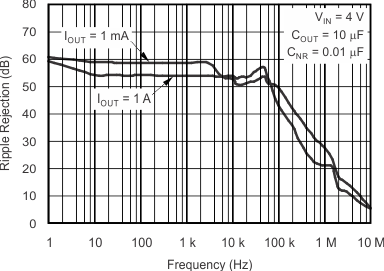
- High PSRR (53 dB at 10 kHz)
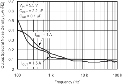
- Ultralow-Noise (40 μVRMS, TPS79630)
- Fast Start-Up Time (50 μs)
- Stable With a 1-μF Ceramic Capacitor
- Excellent Load and Line Transient Response
- Very Low Dropout Voltage (250 mV at Full Load, TPS79630)
- 3 × 3 VSON PowerPAD™, SOT223-6, and
TO-263 Packages
2 Applications
- RF: VCOs, Receivers, ADCs
- Audio
- Bluetooth®, Wireless LAN
- Cellular and Cordless Telephones
- Handheld Organizers, PDAs
3 Description
The TPS796 family of low-dropout (LDO) low-power linear voltage regulators features high power-supply rejection ratio (PSRR), ultralow-noise, fast start-up, and excellent line and load transient responses in small outline, 3 × 3 VSON, SOT223-6, and TO-263 packages. Each device in the family is stable with a small, 1-μF ceramic capacitor on the output. The family uses an advanced, proprietary BiCMOS fabrication process to yield extremely low dropout voltages (for example, 250 mV at 1 A). Each device achieves fast start-up times (approximately 50 μs with a 0.001-μF bypass capacitor) while consuming very low quiescent current (265 μA typical). Moreover, when the device is placed in standby mode, the supply current is reduced to less than 1 μA. The TPS79630 exhibits approximately 40 μVRMS of output voltage noise at 3.0-V output, with a 0.1-μF bypass capacitor. Applications with analog components that are noise sensitive, such as portable RF electronics, benefit from the high PSRR, low noise features, and need fast response time.
Device Information(1)
| PART NUMBER | PACKAGE | BODY SIZE (NOM) |
|---|---|---|
| TPS796 | VSON (8) | 3.00 mm × 3.00 mm |
| SOT-223 (6) | 6.50 mm × 3.50 mm | |
| TO-263 (5) | 10.16 mm × 8.42 mm |
Ripple Rejection vs Frequency
TPS79630

Output Spectral Noise Density vs Frequency
TPS79630
