SWCS132 August 2015
Package Options
Mechanical Data (Package|Pins)
- RSK|64
Thermal pad, mechanical data (Package|Pins)
Orderable Information
1 Device Overview
1.1 Features
- Three Variable-Output Voltage Step-Down Controllers
- Wide VIN Range From 5.4 V to 21 V
- Up to 7-A Output Current for BUCK1 (VCC) and BUCK6 (VDDQ), and 11-A for BUCK2 (VGG) Using External FETs
- I2C DVS Control (0.5 V to 1.45 V in 10-mV Steps) for BUCK1 and BUCK2
- Pin-Selectable Dual Output Voltages (1.2 V or 1.35 V) for BUCK6 (VDDQ)
- Three Variable-Output Voltage Synchronous Step-Down Converters
- VIN Range From 4.5 V to 5.5 V
- Up to 3.5 A of Output Current for BUCK3 (VNN) With I2C DVS Control (0.65 V to
1.45 V in 25-mV Steps) - Up to 3 A of Output Current for BUCK4 (V1P05A) and up to 1.5 A of Output Current for BUCK5 (V1P8A)
- Three LDO Regulators With Adjustable Output Voltage
- LDOA1: I2C-Selectable Output Voltage From 1.35 V to 3.3 V for up to 200 mA of Output Current
- LDOA2: I2C-Selectable Output Voltage From 1.05 V, 1.1 V, 1.15 V, and 1.2 V
- LDOA3: I2C-Selectable Output Voltage From
1.1 V, 1.15 V, 1.2 V, and 1.24 V
- VTT LDO for DDR3 and DDR4 Memory Termination
- Three Load Switches With Slew Rate Control
- Up to 300 mA of Output Current With Voltage Drop Less Than 1.5% of Nominal Input Voltage
- RDSON < 96 mΩ at Input Voltage of 1.8 V
- I2C Interface (Device Address 0x5E) Supports Standard Mode (100 kHz), Fast Mode (400 kHz), and Fast Mode Plus (1 MHz)
- 64-Pin, Single-Row, 0.4-mm Pitch QFN Package
1.2 Applications
- 2-, 3-, or 4-Series Cell Li-Ion Battery Powered Products (NVDC or Non-NVDC)
- Tablet, Ultrabook, and Notebook Computers
- Mobile PCs and Mobile Internet Devices
1.3 Description
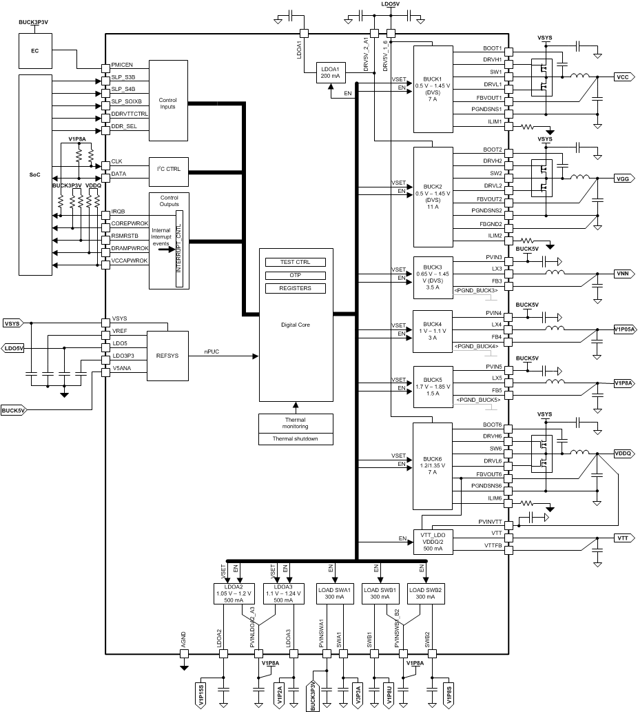
The TPS650842 device is a single-chip solution, power-management IC designed specifically for the latest Intel™ processors targeted for tablets, ultrabooks, and notebooks with NVDC or non-NVDC power architectures, using 2S, 3S, or 4S Li-Ion battery packs. The TPS650842 device is used for essential systems with low-voltage rails merged for the smallest footprint and lowest-cost system-power solution. The TPS650842 device provides the complete power solution based on the Intel Reference Designs. Six highly efficient step-down voltage regulators (VRs), a sink or source LDO (VTT), two LDOs, and three load switches are controlled by power-up sequence logic to provide the proper power rails, sequencing, and protection—including DDR3 and DDR4 memory power. The three regulators (BUCK1–BUCK3) support dynamic voltage scaling (DVS) for maximum efficiency—including support for Connected Standby. The high-frequency VRs use small inductors and capacitors to achieve a small solution size. An I2C interface allows simple control by an embedded controller (EC) or by a system on chip (SoC). The PMIC comes in an 8-mm × 8-mm single-row QFN package with a thermal pad for good thermal dissipation and ease of board routing.
Use the following email address to request the full version of this data sheet: ipgmkt@list.ti.com.
Device Information
| PART NUMBER | PACKAGE | BODY SIZE (NOM) |
|---|---|---|
| TPS650842 | RSK (64) | 8.00 mm × 8.00 mm |
1.4 Functional Block Diagram
