SLVSAQ5E March 2012 – May 2017 TPS62125
PRODUCTION DATA.
- 1 Features
- 2 Applications
- 3 Description
- 4 Revision History
- 5 Pin Configuration and Functions
- 6 Specifications
- 7 Detailed Description
- 8 Application and Implementation
- 9 Power Supply Recommendations
- 10Layout
- 11Device and Documentation Support
- 12Mechanical, Packaging, and Orderable Information
Package Options
Mechanical Data (Package|Pins)
- DSG|8
Thermal pad, mechanical data (Package|Pins)
- DSG|8
Orderable Information
1 Features
- Wide Input Voltage Range 3 V to 17 V
- Input Supply Voltage Supervisor (SVS) With Adjustable Threshold and Hysteresis Consuming Typical 6-µA Quiescent Current
- Wide Output Voltage Range 1.2 V to 10 V
- Typical 13-µA Quiescent Current
- 350-nA Typical Shutdown Current
- Seamless Power Save Mode Transition
- DCS-Control™ Scheme
- Low Output Ripple Voltage
- Up to 1-MHz Switching Frequency
- Highest Efficiency over Wide VIN and VOUT Range
- Pin to Pin Compatible with TPS62160/70
- 100% Duty Cycle Mode
- Power Good Open Drain Output
- Output Discharge Function
- Small 2-mm × 2-mm 8-pin WSON Package
2 Applications
- Embedded Processing
- 4-Cell Alkaline, 1- to 4-Cell Li-Ion Battery-Powered Applications
- 9-V to 15-V Standby Power Supply
- Energy Harvesting
- Inverter (Negative VOUT)
3 Description
The TPS62125 device is a high-efficiency synchronous step-down converter optimized for low and ultralow power applications providing up to 300-mA output current. The wide input voltage range of 3 V to 17 V supports 4-cell alkaline and 1- to 4-cell Li-Ion batteries in series configuration as well as 9-V to 15-V powered applications. The device includes a precise low-power enable comparator which can be used as an input supply voltage supervisor (SVS) to address system specific power-up and power-down requirements. The enable comparator consumes only 6-µA quiescent current and features an accurate threshold of 1.2 V typical as well as an adjustable hysteresis. With this feature, the converter can generate a power supply rail by extracting energy from a storage capacitor fed from high impedance sources such as solar panels or current loops. With its DCS-Control scheme the converter provides power-save mode operation to maintain highest efficiency over the entire load current range. At light loads the converter operates in pulse frequency modulation (PFM) mode and transitions seamlessly and automatically in pulse width modulation (PWM) mode at higher load currents. The DCS-Control™ scheme is optimized for low-output ripple voltage in PFM mode in order to reduce output noise to a minimum and features excellent AC load regulation. An open-drain power good output indicates once the output voltage is in regulation.
Device Information(1)
| PART NUMBER | PACKAGE | BODY SIZE (NOM) |
|---|---|---|
| TPS62125 | WSON (8) | 2.00 mm × 2.00 mm |
- For all available packages, see the orderable addendum at the end of the data sheet.
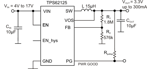
Typical Application Schematic

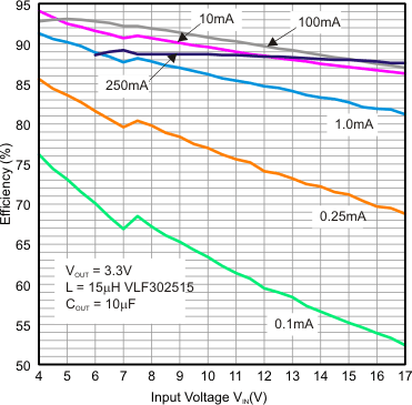
Efficiency vs Input Voltage
