SLVSA95B March 2010 – July 2015 TPS62060 , TPS62061 , TPS62063
PRODUCTION DATA.
- 1 Features
- 2 Applications
- 3 Description
- 4 Revision History
- 5 Device Comparison Table
- 6 Pin Configuration and Functions
- 7 Specifications
- 8 Detailed Description
- 9 Application and Implementation
- 10Power Supply Recommendations
- 11Layout
- 12Device and Documentation Support
- 13Mechanical, Packaging, and Orderable Information
Package Options
Mechanical Data (Package|Pins)
- DSG|8
Thermal pad, mechanical data (Package|Pins)
- DSG|8
Orderable Information
1 Features
- 3-MHz Switching Frequency
- VIN Range from 2.7 V to 6 V
- 1.6-A Output Current
- Up to 97% Efficiency
- Power Save Mode and 3-MHz Fixed PWM Mode
- Output Voltage Accuracy in PWM Mode ±1.5%
- Output Discharge Function
- Typical 18-µA Quiescent Current
- 100% Duty Cycle for Lowest Dropout
- Voltage Positioning
- Clock Dithering
- Supports Maximum 1-mm Height Solutions
- Available in a 2 mm × 2 mm × 0.75 mm WSON
2 Applications
- Point of Load (POL)
- Notebooks, Pocket PCs
- Portable Media Players
- DSP Supplies
3 Description
The TPS6206x is a family of highly efficient synchronous step-down DC-DC converters. They provide up to 1.6-A output current.
With an input voltage range of 2.7 V to 6 V, the device is a perfect fit for power conversion from a single Li-Ion battery as well from 5-V or 3.3-V system supply rails. The TPS6206x operates at 3-MHz fixed frequency and enters power save mode operation at light load currents to maintain high efficiency over the entire load current range. The power save mode is optimized for low output voltage ripple. For low noise applications, the device can be forced into fixed frequency PWM mode by pulling the MODE pin high.
In the shutdown mode, the current consumption is reduced to less than 1 µA and an internal circuit discharges the output capacitor.
TPS6206x family is optimized for operation with a tiny 1-µH inductor and a small 10-µF output capacitor to achieve smallest solution size and high regulation performance.
The TPS6206x operates over a free air temperature of –40°C to 85°C. The device is available in a small 2-mm × 2-mm × 0.75-mm 8-pin WSON PowerPAD™ integrated circuit package.
Device Information(1)
| PART NUMBER | PACKAGE | BODY SIZE (NOM) |
|---|---|---|
| TPS62060 TPS62061 TPS62063 |
WSON (8) | 2.00 mm × 2.00 mm |
- For all available packages, see the orderable addendum at the end of the data sheet.
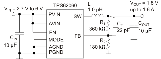
Typical Application Schematic

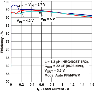
Efficiency vs Load Current
