SLVSDM0 June 2016 TPS61021A
PRODUCTION DATA.
- 1 Features
- 2 Applications
- 3 Description
- 4 Revision History
- 5 Pin Configuration and Functions
- 6 Specifications
- 7 Detailed Description
- 8 Application and Implementation
- 9 Power Supply Recommendations
- 10Layout
- 11Device and Documentation Support
- 12Mechanical, Packaging, and Orderable Information
Package Options
Mechanical Data (Package|Pins)
- DSG|8
Thermal pad, mechanical data (Package|Pins)
- DSG|8
Orderable Information
1 Features
- Input Voltage Range: 0.5 V to 4.4 V
- 0.9 V Minimum Input Voltage for Startup
- Output Voltage Setting Range: 1.8 V to 4.0 V
- 91% Efficiency at VIN = 2.4 V, VOUT = 3.3 V and IOUT = 1.5 A
- 2.0-MHz Switching Frequency
- IOUT > 1.5 A at VOUT = 3.3 V when VIN > 1.8 V
- 17-µA Typical Quiescent Current
- ±2.5% Reference Voltage Accuracy over -40°C to 125°C
- PFM Operation Mode at Light Load
- True Disconnection Between Input and Output During Shutdown
- Output Over Voltage Protection
- Output Short Circuit Protection
- Thermal Shutdown Protection
- 2-mm x 2-mm WSON Package
2 Applications
- Battery Powered IoT Devices
- Gaming Control
- Thermostat
- Portable Medical Equipment
- Supercap Backup System
3 Description
The TPS61021A provides a power supply solution for portable or smart devices powered by alkaline, NiMH, Li-Mn, or Li-ion batteries. The TPS61021A is capable of outputting 3.3-V voltage and 1.5-A current from a battery discharged to as low as 1.8 V. Capable of operating with 0.5-V input voltage enables the TPS61021A to extend the battery run time.
The TPS61021A operates at 2-MHz switching frequency at heavy load and enters power-save mode at light load to maintain high efficiency over the entire load current range. The device only consumes a 17-μA quiescent current from VOUT in light load condition. During shutdown, the load is completely disconnected from the input. In addition, The TPS61021A provides 4.35-V output overvoltage protection, output short circuit protection, and thermal shutdown protection.
The TPS61021A offers a very small solution size due to low count of external components. It allows the use of small inductors and output capacitors with the 2-MHz switching frequency.
The TPS61021A is available in 2.0-mm x 2.0-mm WSON package.
Device Information(1)
| PART NUMBER | PACKAGE | BODY SIZE (NOM) |
|---|---|---|
| TPS61021A | WSON (8) | 2.00-mm x 2.00-mm |
- For all available packages, see the orderable addendum at the end of the datasheet.
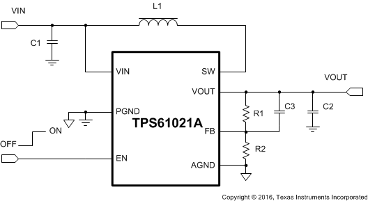
Typical Application Circuit
