SLVS273A February 2000 – November 2015 TPS60140 , TPS60141
PRODUCTION DATA.
- 1 Features
- 2 Applications
- 3 Description
- 4 Revision History
- 5 Description (continued)
- 6 Device Comparison Table
- 7 Pin Configuration and Functions
- 8 Specifications
- 9 Detailed Description
- 10Application and Implementation
- 11Power Supply Recommendations
- 12Layout
- 13Device and Documentation Support
- 14Mechanical, Packaging, and Orderable Information
Package Options
Mechanical Data (Package|Pins)
- PWP|20
Thermal pad, mechanical data (Package|Pins)
- PWP|20
Orderable Information
1 Features
- Regulated 5 V ±4% Output Voltage
- Up to 100-mA Output Current
- 1.8-V to 3.6-V Input Voltage Range
- 65-µA Quiescent Supply Current
- 0.05-µA Shutdown Current, Battery Is Isolated From Load in Shutdown
- Integrated Low-Battery or Power-Good Indicator
- Low-Output Voltage Ripple Over Complete Output Current Range
- Easy-to-Design With Low-EMI Power Supply Because No Inductors Are Required
- Evaluation Module Available (TPS60140EVM-144)
- Available in a 6.5-mm × 4.4-mm 20-Pin HTSSOP Package
2 Applications
- Replacement of DC-DC Converters With Inductors in Battery-Powered Applications:
- Two Battery Cells to 5-V Conversions
- Portable Instruments
- Miniature Equipment
- Backup-Battery Boost Converters
- Medical Instruments
- 5-V Smart Card Supplies
3 Description
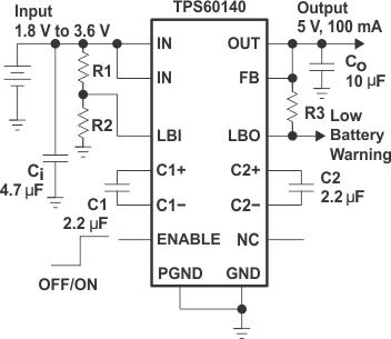
The TPS6014x step-up, regulated charge pumps generate a 5-V ±4% output voltage from a 1.8-V to 3.6-V input voltage range. The devices are typically powered by two alkaline, NiCd, or NiMH battery cells and provide an output current of minimum 100 mA from a 2-V input. Only four external capacitors are needed to build a complete voltage tripler charge pump.
The devices regulate the output by using the pulse-skip topology. The controller is optimized for lowest output voltage ripple over the complete output current range. The output peak current and therefore the output voltage ripple are drastically reduced compared to a conventional pulse-skip topology by regulating the charge pump output resistance. At light loads the maximum output resistance is limited to assure a low quiescent current.
The TPS60140 includes a low-battery comparator that issues a warning if the battery voltage drops below a user-adjustable threshold voltage. The TPS60141 features a power-good output that goes active when the output voltage reaches 90% of its nominal value.
Device Information(1)
| PART NUMBER | PACKAGE | BODY SIZE (NOM) |
|---|---|---|
| TPS6014x | HTSSOP (20) | 6.50 mm × 4.40 mm |
- For all available packages, see the orderable addendum at the end of the data sheet.
Typical Application Schematic

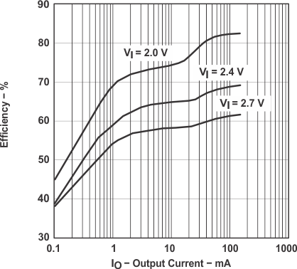
Efficiency vs Output Current
