SLVSCD5D November 2014 – February 2016 TPS54335-1A , TPS54335A , TPS54336A
PRODUCTION DATA.
- 1 Features
- 2 Applications
- 3 Description
- 4 Revision History
- 5 Pin Configuration and Functions
- 6 Specifications
-
7 Detailed Description
- 7.1 Overview
- 7.2 Functional Block Diagram
- 7.3
Feature Description
- 7.3.1 Fixed-Frequency PWM Control
- 7.3.2 Light-Load Operation
- 7.3.3 Voltage Reference
- 7.3.4 Adjusting the Output Voltage
- 7.3.5 Enabling and Adjusting Undervoltage Lockout
- 7.3.6 Error Amplifier
- 7.3.7 Slope Compensation and Output Current
- 7.3.8 Safe Startup into Pre-Biased Outputs
- 7.3.9 Bootstrap Voltage (BOOT)
- 7.3.10 Adjustable Switching Frequency (TPS54335A Only)
- 7.3.11 Soft-Start (TPS54336A Only)
- 7.3.12 Output Overvoltage Protection (OVP)
- 7.3.13 Overcurrent Protection
- 7.3.14 Thermal Shutdown
- 7.3.15 Small-Signal Model for Loop Response
- 7.3.16 Simple Small-Signal Model for Peak Current-Mode Control
- 7.3.17 Small-Signal Model for Frequency Compensation
- 7.4 Device Functional Modes
-
8 Application and Implementation
- 8.1 Application Information
- 8.2
Typical Applications
- 8.2.1 Design Requirements
- 8.2.2 Detailed Design Procedure
- 8.2.3 Application Curves
- 8.2.4 TPS54336A Typical Application
- 9 Power Supply Recommendations
- 10Layout
- 11Device and Documentation Support
- 12Mechanical, Packaging, and Orderable Information
Package Options
Refer to the PDF data sheet for device specific package drawings
Mechanical Data (Package|Pins)
- DRC|10
- DDA|8
Thermal pad, mechanical data (Package|Pins)
Orderable Information
1 Features
- Synchronous 128-mΩ and 84-mΩ MOSFETs for
3-A Continuous Output Current -
TPS54335A: Internal 2-ms Soft-Start,
50-kHz to 1.5-MHz Adjustable Frequency - TPS54336A: Adjustable Soft-Start,
Fixed 340-kHz Frequency - Low 2-µA Shutdown, Quiescent Current
- 0.8-V Voltage Reference with ±0.8% Accuracy
- Current Mode Control
- Monotonic Startup into Pre-Biased Outputs
- Pulse Skipping for Light-Load Efficiency
- Hiccup Mode Overcurrent Protection
- Thermal Shutdown (TSD) and
Overvoltage Transition Protection - 8-Pin SO PowerPAD™ and 10-Pin VSON Package
- Create a Custom Design Using the TPS54335A with the WEBENCH Power Designer
2 Applications
- Consumer Applications such as a Digital TV (DTV), Set Top Box (STB, DVD/Blu-ray Player), LCD Display, CPE (Cable Modem, WiFi Router), DLP Projectors, Smart Meters
- Battery Chargers
- Industrial and Car Audio Power Supplies
- 5-V, 12-V, and 24-V Distributed Power Bus Supply
3 Description
The TPS5433xA family of devices are synchronous converters with an input-voltage range of 4.5 V to 28 V. These devices include This device has an integrated low-side switching FET that eliminates the need for an external diode which reduces component count.
Efficiency is maximized through the integrated 128-mΩ and 84-mΩ MOSFETs, low IQ and pulse skipping at light loads. Using the enable pin, the shutdown supply current is reduced to 2 μA. This step-down (buck) converter provides accurate regulation for a variety of loads with a well-regulated voltage reference that is 1.5% over temperature.
Cycle-by-cycle current limiting on the high-side MOSFET protects the TPS5433xA family of devices in overload situations and is enhanced by a low-side sourcing current limit which prevents current runaway. A low-side sinking current-limit turns off the low-side MOSFET to prevent excessive reverse current. Hiccup protection is triggered if the overcurrent condition continues for longer than the preset time. Thermal shutdown disables the device when the die temperature exceeds the threshold and enables the device again after the built-in thermal hiccup time.
Device Information(1)
| PART NUMBER | PACKAGE | BODY SIZE (NOM) |
|---|---|---|
| TPS54335A TPS54336A |
SO PowerPAD (8) | 4.89 mm × 3.90 mm |
| VSON (10) | 3.00 mm × 3.00 mm | |
| TPS54335-1A | VSON (10)(2) | 3.00 mm × 3.00 mm |
- For all available packages, see the orderable addendum at the end of the datasheet.
- The DRC package for the TPS54335-1A device has a narrower heat-pad for more clearance between the pins and heat pad. See the Differences Between the Two DRC Packages section.
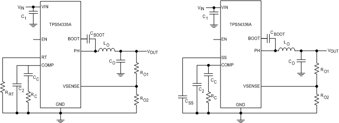
Simplified Schematic
