SLUSB94A OCTOBER 2012 – September 2016 TPS51716
PRODUCTION DATA.
- 1 Features
- 2 Applications
- 3 Description
- 4 Revision History
- 5 Pin Configuration and Functions
- 6 Specifications
-
7 Detailed Description
- 7.1 Overview
- 7.2 Functional Block Diagram
- 7.3
Feature Description
- 7.3.1 VDDQ Switch Mode Power Supply Control
- 7.3.2 VREF and REFIN, VDDQ Output Voltage
- 7.3.3 Soft-Start and Powergood
- 7.3.4 Power State Control
- 7.3.5 VDDQ Overvoltage and Undervoltage Protection
- 7.3.6 VDDQ Out-of-Bound Operation
- 7.3.7 VDDQ Overcurrent Protection
- 7.3.8 VTT and VTTREF
- 7.3.9 VTT Overcurrent Protection
- 7.3.10 V5IN Undervoltage Lockout (UVLO) Protection
- 7.3.11 Thermal Shutdown
- 7.4 Device Functional Modes
- 8 Application and Implementation
- 9 Power Supply Recommendations
- 10Layout
- 11Device and Documentation Support
- 12Mechanical, Packaging, and Orderable Information
Package Options
Mechanical Data (Package|Pins)
- RUK|20
Thermal pad, mechanical data (Package|Pins)
- RUK|20
Orderable Information
1 Features
- Synchronous Buck Controller (VDDQ)
- Conversion Voltage Range: 3 to 28 V
- Output Voltage Range: 0.7 to 1.8 V
- 0.8% VREF Accuracy
- D-CAP2™ Mode for Ceramic Output Capacitors
- Selectable 500-kHz/670-kHz Switching Frequencies
- Optimized Efficiency at Light and Heavy Loads With Auto-Skip Function
- Supports Soft-Off in S4/S5 States
- OCL/OVP/UVP/UVLO Protections
- Powergood Output
- 2-A LDO (VTT), Buffered Reference (VTTREF)
- 2-A (Peak) Sink and Source Current
- Requires Only 10-μF of Ceramic Output Capacitance
- Buffered, Low Noise, 10-mA VTTREF Output
- 0.8% VTTREF, 20-mV VTT Accuracy
- Support High-Z in S3 and Soft-Off in S4/S5
- Thermal Shutdown
- 20-Pin, 3 mm × 3 mm, WQFN Package
2 Applications
3 Description
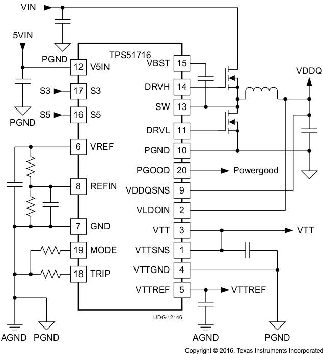
The TPS51716 provides a complete power supply for DDR2, DDR3, DDR3L, LPDDR3, and DDR4 memory systems in the lowest total cost and minimum space. It integrates a synchronous buck regulator controller (VDDQ) with a 2-A sink/source tracking LDO (VTT) and buffered low noise reference (VTTREF). The TPS51716 employs D-CAP2 mode coupled with 500 kHz or 670 kHz operating frequencies that supports ceramic output capacitors without an external compensation circuit. The VTTREF tracks VDDQ/2 with excellent 0.8% accuracy. The VTT, which provides 2-A sink/source peak current capabilities, requires only 10 μF of ceramic capacitance. In addition, the device features a dedicated LDO supply input.
The TPS51716 provides rich, useful functions as well as excellent power supply performance. It supports flexible power state control, placing VTT at high-Z in S3 and discharging VDDQ, VTT and VTTREF (soft-off) in S4/S5 state. It includes programmable OCL with low-side MOSFET RDS(on) sensing, OVP/UVP/UVLO and thermal shutdown protections.
TI offers the TPS51716 in a 20-pin, 3 mm × 3 mm, WQFN package and specifies it for an ambient temperature range between –40°C and 85°C.
Device Information(1)
| PART NUMBER | PACKAGE | BODY SIZE (NOM) |
|---|---|---|
| TPS51716 | WQFN (20) | 3.00 mm × 3.00 mm |
- For all available packages, see the orderable addendum at the end of the data sheet.
Block Diagram

4 Revision History
Changes from * Revision (October 2012) to A Revision
- Added ESD Ratings table, Detailed Description section, Application and Implementation section, Power Supply Recommendations section, Layout section, Device and Documentation Support section, and Mechanical, Packaging, and Orderable Information sectionGo
- Updated the Title From: Complete DDR2, DDR3, DDR3L, and LPDDR3 Memory Power Solution To: Complete DDR2, DDR3, DDR3L, LPDDR3, and DDR4 Memory Power Go
- Changed Applications list From: DDR2/DDR3/DDR3L/LPDDR3 Memory Power Supplies To: DDR2, DDR3, DDR3L, LPDDR3, and DDR4 Memory Power SuppliesGo