SBVS211B August 2012 – April 2015
PRODUCTION DATA.
- 1 Features
- 2 Applications
- 3 Description
- 4 Revision History
- 5 Pin Configuration and Functions
- 6 Specifications
- 7 Detailed Description
- 8 Application and Implementation
- 9 Power Supply Recommendations
- 10Layout
- 11Device and Documentation Support
- 12Mechanical, Packaging, and Orderable Information
Package Options
Mechanical Data (Package|Pins)
- DRY|6
Thermal pad, mechanical data (Package|Pins)
- DRY|6
Orderable Information
1 Features
- Very Small Package: 1.45-mm × 1.00-mm SON
- Operating Range: 1.6 V to 6.5 V
- Single (TPS3422) or Dual (TPS3420 and TPS3421) Push-Button Inputs
- Low Supply Current: 250 nA (Typical)
- Two-State Logic, User-Selectable Input Delay:
- For Example: 7.5 s and 0 s
- Multiple Timing Options Available
-
Fixed Time-out Pulse at RST (TPS3421 and TPS3422): 400 ms (Typical)
- Other Timing Options Available on Request
- Active Low, Open-Drain Output
2 Applications
- Smart Phones
- Tablets, Ultrabooks™
- Gaming Consoles
- Portable Consumers
- Navigation Devices
- Consumer Medical
- Toys
3 Description
The TPS3420, TPS3421, and TPS3422 (TPS342x) are low-current, ultrasmall, push-button reset timers. These devices use a long timing setup delay to provide the intended system reset, and avoid resets from short push-button closures or key presses. This reset configuration also allows for differentiation between software interrupts and hard system resets.
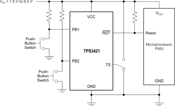
The TPS3420 and TPS3421 monitor two inputs (PB1 and PB2) and output an active-low reset pulse signal (RST) when both inputs are low for the selected time delay. For the TPS3421, RST remains low for a factory-programmed fixed time. For the TPS3420, RST remains low until one of the PBx inputs is released. The need for a dedicated reset button is eliminated because two inputs are used to ensure reset. The TPS3422 monitors one input (PB1) and outputs an active-low reset pulse signal (RST) when PB1 is low for the selected time delay.
The TPS342x have an open-drain output that can be wire-ORed with other open-drain devices. The TPS342x operate from 1.6 V to 6.5 V over the –40°C to +125°C temperature range, and provide a precise, space-conscious micropower solution for system resetting needs.
Device Information(1)
| PART NUMBER | PACKAGE | BODY SIZE (NOM) |
|---|---|---|
| TPS342x | USON (6) | 1.45 mm × 1.00 mm |
- For all available packages, see the orderable addendum at the end of the data sheet.
TPS3421 Typical Application Diagram

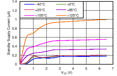
Standby Supply Current vs Supply Voltage
