SLVSCF3A June 2014 – March 2015
PRODUCTION DATA.
- 1 Features
- 2 Applications
- 3 Description
- 4 Simplified Schematic
- 5 Revision History
- 6 Pin Configuration and Functions
- 7 Specifications
- 8 Parametric Measurement Information
-
9 Detailed Description
- 9.1 Overview
- 9.2 Functional Block Diagram
- 9.3
Feature Description
- 9.3.1 Enable and Adjusting Undervoltage Lockout
- 9.3.2 Overvoltage Protection (OVP)
- 9.3.3 Hot Plug-in and In-Rush Current Control
- 9.3.4 Overload and Short Circuit Protection :
- 9.3.5 FAULT Response
- 9.3.6 Current Monitoring:
- 9.3.7 Power Good Comparator
- 9.3.8 IN, OUT and GND Pins
- 9.3.9 Thermal Shutdown:
- 9.4 Device Functional Modes
-
10Application and Implementation
- 10.1 Application Information
- 10.2
Typical Application
- 10.2.1
eFuse for Enterprise SSDs
- 10.2.1.1 Design Requirements
- 10.2.1.2
Detailed Design Procedure
- 10.2.1.2.1 Step by Step Design Procedure
- 10.2.1.2.2 Programming the Current-Limit Threshold: R(ILIM) Selection
- 10.2.1.2.3 Undervoltage Lockout and Overvoltage Set Point
- 10.2.1.2.4 Programming Current Monitoring Resistor - RIMON
- 10.2.1.2.5 Setting Output Voltage Ramp time (tdVdT)
- 10.2.1.2.6 Programing the Power Good Set Point
- 10.2.1.2.7 Support Component Selections - R6, R7 and CIN
- 10.2.1.3 Application Curves
- 10.2.1
eFuse for Enterprise SSDs
- 10.3 System Examples
- 11Power Supply Recommendations
- 12Layout
- 13Device and Documentation Support
- 14Mechanical, Packaging, and Orderable Information
Package Options
Refer to the PDF data sheet for device specific package drawings
Mechanical Data (Package|Pins)
- RVC|20
Thermal pad, mechanical data (Package|Pins)
Orderable Information
1 Features
- 2.7 V – 18 V Operating Voltage, 20 V (Max)
- 42 mΩ RON (Typical)
- 0.6 A to 5.3 A Adjustable Current Limit (±8%)
- IMON Current Indicator Output (±8%)
- 200 μA Operating IQ (Typical)
- 95 μA DevSleep Mode IQ (Typical)
- 15 μA Disabled IQ (Typical)
- ±2% Overvoltage, Undervoltage Threshold
- Reverse Current Blocking
- 1 μs Reverse Voltage Shutoff
- Programmable dVo/dt Control
- Power Good and Fault Outputs
- -40°C to 125°C Junction Temperature Range
- UL 2367 Recognized
- File No. 169910
- RILIM ≥ 20 kΩ (4.81 A max)
- UL60950 - Safe during Single Point Failure Test
- Open/Short ILIM detection
2 Applications
- PCIe/SATA/SAS HDD and SSD Drives
- Enterprise and Micro Servers
- Smart Load Switch
- Set-Top-Box (STB), DTVs and Game Consoles
- RAID Cards - Holdup Power Management
- Telecom Switches and Routers
- Adapter Powered Devices
3 Description
The TPS25940 eFuse Power Switch is a compact, feature rich power management device with a full suite of protection functions, including a low power DevSleep™ mode that supports compliance with the SATA™ Device Sleep standard. The wide operating range allows control of many popular DC bus voltages. Integrated back to back FETs provide bidirectional current control making the device well suited for systems with load side holdup energy that must not drain back to a failed supply bus.
Load, source and device protection are provided with many programmable features including overcurrent, dVo/dt ramp and overvoltage, undervoltage thresholds. For system status monitoring and downstream load control, the device provides PGOOD, FLT and precise current monitor output. Precise programmable undervoltage, overvoltage thresholds and the low IQ DevSleep mode simplify SSD power management design.
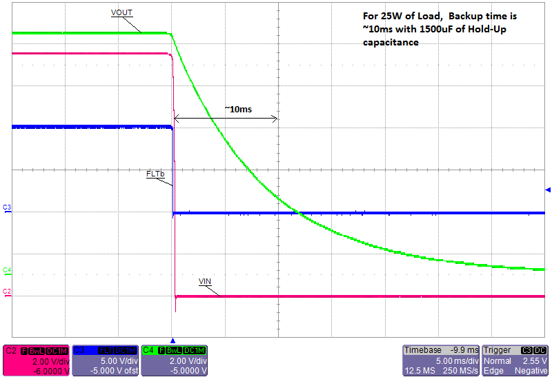
The TPS25940 monitors V(IN) and V(OUT) to provide true reverse current blocking when V(IN) < (V(OUT) - 10 mV). This function supports swift changeover to a boosted voltage energy storage element in systems where backup voltage is greater than bus voltage.
Device Information(1)
| PART NUMBER(2) | PACKAGE | BODY SIZE (NOM) |
|---|---|---|
| TPS25940A | WQFN (20) | 3.00 mm x 4.00 mm |
| TPS25940L |
- For all available packages, see the orderable addendum at the end of the datasheet.
- TPS25940L = Latched, TPS25940A = Auto Retry
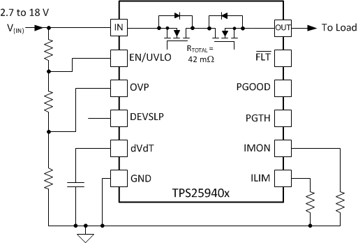
4 Simplified Schematic

Power Fail Detection and Blocking
