SLUSCP2 September 2016 TPS2549
PRODUCTION DATA.
- 1 Features
- 2 Applications
- 3 Description
- 4 Revision History
- 5 Pin Configuration and Functions
- 6 Specifications
- 7 Parameter Measurement Information
-
8 Detailed Description
- 8.1 Overview
- 8.2 Functional Block Diagram
- 8.3 Feature Description
- 8.4 Device Functional Modes
- 9 Application and Implementation
- 10Power Supply Recommendations
- 11Layout
- 12Device and Documentation Support
- 13Mechanical, Packaging, and Orderable Information
Package Options
Mechanical Data (Package|Pins)
- RTE|16
Thermal pad, mechanical data (Package|Pins)
- RTE|16
Orderable Information
1 Features
- 4.5-V to 6.5-V Operating Range
- 47-mΩ (typical) High-Side MOSFET
- 3-A Maximum Continuous Output Current
- ±5% CS Output for Cable Compensation
- CDP Mode per USB Battery Charging Specification 1.2
- Automatic DCP Modes Selection:
- Shorted Mode per BC1.2 and YD/T 1591-2009
- 2.7-V Divider 3 Mode
- 1.2-V Mode
- D+ and D– Client Mode for System Update
- D+ and D– Short-to-VBUS Protection
- D+ and D– ±8-kV Contact and ±15-kV Air Discharge ESD Rating (IEC 61000-4-2)
- UL Recognition and CB Certification Pending
- –40°C to 125°C Junction Operating Temperature
- 16-Pin QFN (3-mm × 3-mm) Package
2 Applications
- USB Ports (Host and Hubs)
- Wall Charging Adapters
- Aftermarket Automotive Chargers
3 Description
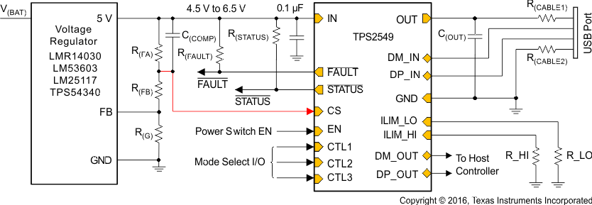
The TPS2549 device is a USB charging port controller and power switch with a current-sense output that is able to control an upstream supply. This allows it to maintain 5 V at the USB port even with heavy
heavy charging currents. This is important in systems with long USB cables where significant voltage drops can occur while fast-charging portable devices.
The TP2549 47-mΩ power switch has two selectable, programmable current limits that support port power management by providing a lower current limit that can be used when adjacent ports are experiencing heavy loads. This is important in systems with multiple ports and an upstream supply unable to provide full current to all ports simultaneously.
The DCP_Auto scheme detects and selects the proper D+ and D– settings to communicate with the attached device, so that it can fast-charge at full current. The integrated CDP detection enables up to 1.5-A fast charging of most portable devices with simultaneous data communication.
The unique client-mode feature allows software updates to client devices, but avoids power conflicts by turning off the internal power switch while keeping the data line connection.
Additionally, the TPS2549 device integrates short-to-VBUS protection for D+ and D– to prevent damage when D+ and/or D– unexpectedly short to VBUS. To save space in the application, the TPS2549 device also integrates ESD protection to pass IEC61000-4-2 without external circuitry on D+ and D–.
Device Information(1)
| PART NUMBER | PACKAGE | BODY SIZE (NOM) |
|---|---|---|
| TPS2549 | WQFN (16) | 3.00 mm × 3.00 mm |
- For all available packages, see the orderable addendum at the end of the data sheet.
Simplified Schematic
