SCPS164D MAY 2007 – February 2017 TCA6507
PRODUCTION DATA.
- 1 Features
- 2 Applications
- 3 Description
- 4 Revision History
- 5 Pin Configuration and Functions
- 6 Specifications
- 7 Parameter Measurement Information
-
8 Detailed Description
- 8.1 Overview
- 8.2 Functional Block Diagram
- 8.3 Feature Description
- 8.4 Device Functional Modes
- 8.5 Programming
- 8.6
Register Maps
- 8.6.1 Registers 0x00 - 0x02 (Select Registers)
- 8.6.2 Register 0x03 (Fade-ON Time)
- 8.6.3 Register 0x04 (Fully-ON Time)
- 8.6.4 Register 0x05 (Fade-OFF Time)
- 8.6.5 Register 0x06 - 0x07 (Fully-OFF Time)
- 8.6.6 Register 0x08 (Maximum Intensity per Bank)
- 8.6.7 Register 0x09 (One-Shot / Master Intensity)
- 8.6.8 Register 0x0A (Initialization Register)
- 9 Application and Implementation
- 10Power Supply Recommendations
- 11Layout
- 12Device and Documentation Support
- 13Mechanical, Packaging, and Orderable Information
Package Options
Mechanical Data (Package|Pins)
Thermal pad, mechanical data (Package|Pins)
- RUE|12
Orderable Information
1 Features
- Seven LED Driver Outputs: ON, OFF, Blinking, Fading at Programmable Rates
- Open-Drain Outputs Directly Drive LEDs to
40-mA Maximum - Two Independent Banks of LED Drivers
- Widely Programmable Blink Rates, Fade-ON and Fade-OFF Rates and Maximum Intensity
- Outputs Not Used as LED Drivers Can Be Used as Regular General-Purpose Open-Drain Outputs
- 16 Steps of Maximum Intensity Control from
Fully-OFF to Fully-ON States - Smooth Perceived Transitions for Fade-ON and Fade-OFF
- Operating Power-Supply Voltage Range of
1.65 V to 3.6 V - 5.5-V Tolerant Open-Drain Outputs
- Low Standby Current With Shutdown Capability for Additional Power Savings
- Programmed Through I2C Bus Interface Logic Compatible With SMBus
- No Glitch on Power Up
- ESD Protection Exceeds JESD 22
- 2000-V Human-Body Model (A114-A)
- 200-V Machine Model (A115-A)
- 1000-V Charged-Device Model (C101)
- Latch-Up Performance Exceeds 100 mA Per JESD 78, Class II
2 Applications
- Mobile Phones
- Desktop and Laptop Computers
- Human Machine Interface
3 Description
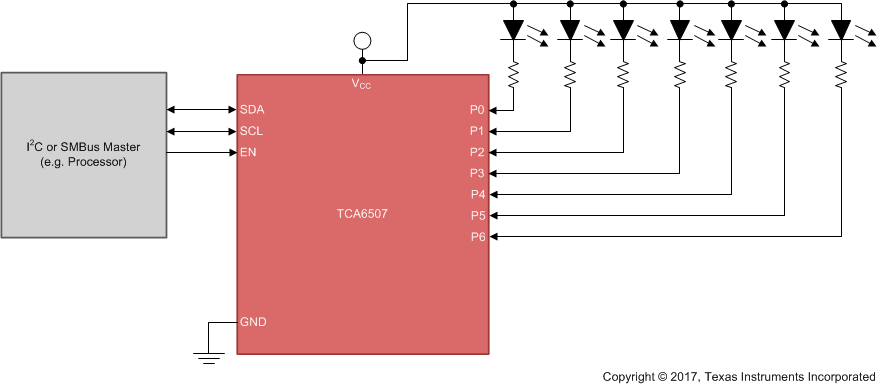
This 7-bit LED dimmer for the two-line bidirectional bus (I2C) is designed to control (or dim) LEDs through the I2C interface. Without this device, the microcontroller must be actively involved in turning on and off the LEDs (per the required dimming rate), which uses valuable processor time. The TCA6507 alleviates this issue by limiting the number of operations required by the processor in blinking LEDs and helps to create a more efficient system. The TCA6507 handles all pulse width modulation (PWM) logic, allowing the processor to use its cycles for more important tasks.
Device Information(1)
| PART NUMBER | PACKAGE | BODY SIZE (NOM) |
|---|---|---|
| TCA6507 | TSSOP (14) | 5.00 mm × 4.40 mm |
| BGA MICROSTAR JUNIOR (12) | 2.00 mm × 2.50 mm | |
| X2QFN (12) | 2.00 mm × 1.40 mm |
- For all available packages, see the orderable addendum at the end of the data sheet.
Simplified Schematic
