SBOS376I November 2006 – July 2016 OPA827
PRODUCTION DATA.
- 1 Features
- 2 Applications
- 3 Description
- 4 Revision History
- 5 Pin Configuration and Functions
- 6 Specifications
- 7 Detailed Description
- 8 Application and Implementation
- 9 Power Supply Recommendations
- 10Layout
- 11Device and Documentation Support
- 12Mechanical, Packaging, and Orderable Information
Package Options
Mechanical Data (Package|Pins)
Thermal pad, mechanical data (Package|Pins)
Orderable Information
1 Features
- Input Voltage Noise Density:
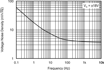
4 nV/√Hz at 1 kHz - Input Voltage Noise:
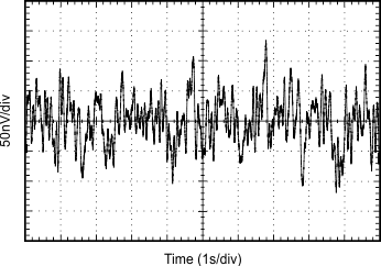
0.1 Hz to 10 Hz: 250 nVPP - Input Bias Current: 10 pA (Maximum)
- Input Offset Voltage: 150 µV (Maximum)
- Input Offset Drift: 2 µV/°C (Maximum)
- Gain Bandwidth: 22 MHz
- Slew Rate: 28 V/µs
- Quiescent Current: 4.8 mA/Ch
- Wide Supply Range: ±4 V to ±18 V
- Packages: 8-Pin SOIC and 8-Pin VSSOP
2 Applications
- ADC Drivers
- DAC Output Buffers
- Test Equipment
- Medical Equipment
- PLL Filters
- Seismic Applications
- Transimpedance Amplifiers
- Integrators
- Active Filters
3 Description
The OPA827 series of JFET operational amplifiers combine outstanding DC precision with excellent AC performance. These amplifiers offer low offset voltage (150 µV, maximum), very low drift over temperature (0.5 µV/°C, typical), low-bias current (3 pA, typical), and very low 0.1-Hz to 10-Hz noise (250 nVPP, typical). The device operates over a wide supply voltage range, ±4 V to ±18 V on a low supply current (4.8 mA/Ch, typical).
Excellent AC characteristics, such as a 22-MHz gain bandwidth product (GBW), a slew rate of 28 V/µs, and precision DC characteristics make the OPA827 series well-suited for a wide range of applications including 16-bit to 18-bit mixed signal systems, transimpedance (I/V-conversion) amplifiers, filters, precision ±10-V front ends, and professional audio applications.
The OPA827 is available in both 8-pin SOIC and 8-pin VSSOP surface-mount packages, and is specified from –40°C to 125°C.
Device Information(1)
| PART NUMBER | PACKAGE | BODY SIZE (NOM) |
|---|---|---|
| OPA827 | SOIC (8) | 4.90 mm × 3.91 mm |
| VSSOP (8) | 3.00 mm × 3.00 mm |
- For all available packages, see the orderable addendum at the end of the data sheet.
Input Voltage Noise Density vs Frequency

0.1-Hz to 10-Hz Noise
