SLOS805C July 2012 – August 2016 OPA1662-Q1
PRODUCTION DATA.
- 1 Features
- 2 Applications
- 3 Description
- 4 Revision History
- 5 Description Continued
- 6 Pin Configuration and Functions
- 7 Specifications
- 8 Detailed Description
- 9 Application and Implementation
- 10Power Supply Recommendations
- 11Layout
- 12Device and Documentation Support
- 13Mechanical, Packaging, and Orderable Information
Package Options
Mechanical Data (Package|Pins)
Thermal pad, mechanical data (Package|Pins)
Orderable Information
1 Features
- Qualified for Automotive Applications
- AEC-Q100 Qualified With the Following Results
- Low Noise: 3.3 nV/√Hz at 1 kHz
- Low Distortion: 0.00006% at 1 kHz
- Low Quiescent Current: 1.5 mA per Channel
- Slew Rate: 17 V/μs
- Wide Gain Bandwidth: 22 MHz (G = 1)
- Unity Gain Stable
- Rail-to-Rail Output
- Wide Supply Range: ±1.5 V to ±18 V,
or 3 V to 36 V - Small Package Sizes:
Dual: 8-Pin SOIC and VSSOP
2 Applications
- Automotive
- Car Audio
- Premium Audio
- External Audio Amplifiers
- Body Control Modules
3 Description
The OPA1662-Q1 is a dual, bipolar-input operational amplifier which is well suited for premium audio external amplifier applications in infotainment and cluster systems. In audio systems, the main concern is to ensure a clear, quality output signal which means minimuzing any noise introduced to the signal. The OPA1662-Q1 offers low noise density with an ultra-low distortion of 0.00006% at 1 kHz that maximizes the signal output. Additionally, this op amp offers rail-to-rail output swing to within 600 mV with 2-kΩ load. The wide headroom ensures that the output signal does not clip, and therefore preserves the audio quality.
the OPA1662-Q1 operates over a very wide supply range of ±1.5 V to ±18 V, or 3 V to 36 V, on only 1.5 mA of supply current per channel. The wide supply range enables design flexibility for the device as it can be integrated from a power amplifier driven by the battery to being driven from an ADC to DAC for low-power applications. Additionally, this device also has a high-output drive capability of ±30 mA and can act as the sole audio amplifier for low-power applications, such as for cluster chimes.
Device Information(1)
| PART NUMBER | PACKAGE | BODY SIZE (NOM) |
|---|---|---|
| OPA1662-Q1 | SOIC (8) | 4.90 mm × 3.91 mm |
| VSSOP (8) | 3.00 mm × 3.00 mm |
- For all available packages, see the orderable addendum at the end of the data sheet.
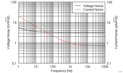
Input Voltage Noise Density and Input Current Noise Density vs Frequency

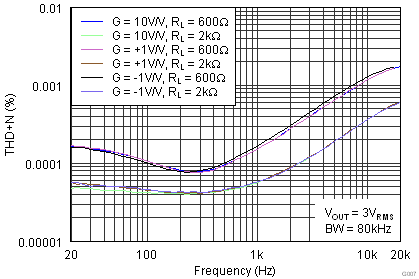
THD+N Ratio vs Frequency
