SNVSCH4 December 2022 LP8769-Q1
PRODUCTION DATA
- 1Features
- 2Applications
- 3Description
- 4Revision History
- 5Pin Configuration and Functions
- 6Device and Documentation Support
- 7Mechanical, Packaging, and Orderable Information
Package Options
Mechanical Data (Package|Pins)
- RQK|32
Thermal pad, mechanical data (Package|Pins)
Orderable Information
1 Features
- AEC-Q100 Qualified with the
following results:
- Input voltage: 2.8 V to 5.5 V
- Device temperature grade 1: –40°C to +125°C ambient operating temperature range
- Device HBM ESD classification Level 2
- Device CDM ESD classification Level C4B
- Functional Safety-Compliant
- Developed for functional safety applications
- Documentation available to aid ISO 26262 system design up to ASIL-D
- Documentation available to aid IEC 61508 system design up to SIL-3
- Systematic capability up to ASIL-D
- Hardware integrity up to ASIL-D
- Windowed voltage and over-current monitors
- Watchdog with selectable trigger / Q&A mode
- Level or PWM error signal monitoring (ESM)
- Thermal monitoring with high temperature warning and thermal shutdown
- Bit-integrity (CRC) error detection on configuration registers and non-volatile memory
- 4 high-efficiency step-down DC/DC
converters:
- Output voltage: 0.3 V to 3.34 V (0.3 V to 1.9 V for multi-phase outputs)
- Maximum output current: 5 A per phase, up to 20 A with 4-phase configuration
- Programmable output voltage slew-rate: 0.5 mV/µs to 33 mV/µs
- Switching frequency: 2.2 MHz or 4.4 MHz
- 10 configurable general purpose I/O (GPIO)
- SPMI interface for multi-PMIC synchronization
- Input overvoltage monitor (OVP) and undervoltage lockout (UVLO)
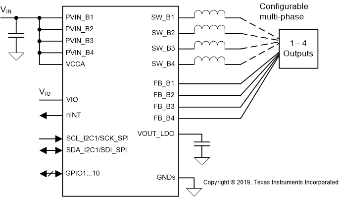
 Simplified Schematic