SNVS324K January 2005 – January 2016 LP38691-ADJ , LP38691-ADJ-Q1 , LP38693-ADJ , LP38693-ADJ-Q1
PRODUCTION DATA.
- 1 Features
- 2 Applications
- 3 Description
- 4 Revision History
- 5 Pin Configuration and Functions
- 6 Specifications
- 7 Detailed Description
-
8 Application and Implementation
- 8.1 Application Information
- 8.2
Typical Applications
- 8.2.1 Design Requirements
- 8.2.2 Detailed Design Procedure
- 8.2.3 Application Curve
- 9 Power Supply Recommendations
- 10Layout
- 11Device and Documentation Support
- 12Mechanical, Packaging, and Orderable Information
Package Options
Mechanical Data (Package|Pins)
- NGG|6
Thermal pad, mechanical data (Package|Pins)
Orderable Information
1 Features
- Wide Input Voltage Range: 2.7 V to 10 V
- All WSON Options are Available as AEC-Q100 Grade 1
- Output Voltage Range: 1.25 V to 9 V
- 2% Adjust (ADJ) Pin Voltage Accuracy (25°C)
- Low Dropout Voltage: 250 mV at 500 mA
(Typical, 5-V Out) - Precision (Trimmed) Bandgap Reference
- Ensured Specs for –40°C to +125°C
- 1-µA Off-State Quiescent Current
- Thermal Overload Protection
- Foldback Current Limiting
- Ground (GND) Pin Current: 55 µA (Typical) at Full Load
- Enable (EN) Pin (LP38693-ADJ)
2 Applications
- Hard Disk Drives
- Notebook Computers
- Battery-Powered Devices
- Portable Instrumentation
3 Description
The LP3869x-ADJ low-dropout CMOS linear regulators provide 2% precision reference voltage, extremely low dropout voltage (250 mV at 500-mA load current, VOUT = 5 V), and excellent AC performance using ultra-low equivalent series resistance (ESR) ceramic output capacitors.
The low thermal resistance of the WSON and SOT-223 packages allow use of the full operating current even in high ambient temperature environments.
The use of a PMOS power transistor means that no DC base drive current is required to bias it, thus allowing the GND-pin current to remain below 100 µA regardless of load current, input voltage, or operating temperature.
Device Information(1)
| PART NUMBER | PACKAGE | BODY SIZE (NOM) |
|---|---|---|
| LP38691-ADJ | WSON (6) | 3.00 mm × 3.00 mm |
| LP38693-ADJ | SOT-223 (5) | 6.50 mm × 3.56 mm |
| WSON (6) | 3.00 mm × 3.00 mm |
- For all available packages, see the orderable addendum at the end of the data sheet.
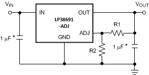
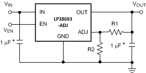
Typical Application Circuits

