SNAS674B September 2015 – February 2017 LMK61E2
PRODUCTION DATA.
- 1 Features
- 2 Applications
- 3 Description
- 4 Revision History
- 5 Pin Configuration and Functions
-
6 Specifications
- 6.1 Absolute Maximum Ratings
- 6.2 ESD Ratings
- 6.3 Recommended Operating Conditions
- 6.4 Thermal Information
- 6.5 Electrical Characteristics - Power Supply
- 6.6 LVPECL Output Characteristics
- 6.7 LVDS Output Characteristics
- 6.8 HCSL Output Characteristics
- 6.9 OE Input Characteristics
- 6.10 ADD Input Characteristics
- 6.11 Frequency Tolerance Characteristics
- 6.12 Power-On/Reset Characteristics (VDD)
- 6.13 I2C-Compatible Interface Characteristics (SDA, SCL)
- 6.14 PSRR Characteristics
- 6.15 Other Characteristics
- 6.16 PLL Clock Output Jitter Characteristics
- 6.17 Typical 156.25-MHz Output Phase Noise Characteristics
- 6.18 Typical 161.1328125 MHz Output Phase Noise Characteristics
- 6.19 Additional Reliability and Qualification
- 6.20 Typical Characteristics
- 7 Parameter Measurement Information
-
8 Detailed Description
- 8.1 Overview
- 8.2 Functional Block Diagram
- 8.3
Feature Description
- 8.3.1 Device Block-Level Description
- 8.3.2 Device Configuration Control
- 8.3.3 Register File Reference Convention
- 8.3.4 Configuring the PLL
- 8.3.5 Integrated Oscillator
- 8.3.6 Reference Doubler
- 8.3.7 Phase Frequency Detector
- 8.3.8 Feedback Divider (N)
- 8.3.9 Fractional Circuitry
- 8.3.10 Charge Pump
- 8.3.11 Loop Filter
- 8.3.12 VCO Calibration
- 8.3.13 High-Speed Output Divider
- 8.3.14 High-Speed Clock Output
- 8.3.15 Device Status
- 8.4 Device Functional Modes
- 8.5 Programming
- 8.6 EEPROM Map
- 8.7
Register Map
- 8.7.1
Register Descriptions
- 8.7.1.1 VNDRID_BY1 Register; R0
- 8.7.1.2 VNDRID_BY0 Register; R1
- 8.7.1.3 PRODID Register; R2
- 8.7.1.4 REVID Register; R3
- 8.7.1.5 SLAVEADR Register; R8
- 8.7.1.6 EEREV Register; R9
- 8.7.1.7 DEV_CTL Register; R10
- 8.7.1.8 XO_CAPCTRL_BY1 Register; R16
- 8.7.1.9 XO_CAPCTRL_BY0 Register; R17
- 8.7.1.10 DIFFCTL Register; R21
- 8.7.1.11 OUTDIV_BY1 Register; R22
- 8.7.1.12 OUTDIV_BY0 Register; R23
- 8.7.1.13 PLL_NDIV_BY1 Register; R25
- 8.7.1.14 PLL_NDIV_BY0 Register; R26
- 8.7.1.15 PLL_FRACNUM_BY2 Register; R27
- 8.7.1.16 PLL_FRACNUM_BY1 Register; R28
- 8.7.1.17 PLL_FRACNUM_BY0 Register; R29
- 8.7.1.18 PLL_FRACDEN_BY2 Register; R30
- 8.7.1.19 PLL_FRACDEN_BY1 Register; R31
- 8.7.1.20 PLL_FRACDEN_BY0 Register; R32
- 8.7.1.21 PLL_MASHCTRL Register; R33
- 8.7.1.22 PLL_CTRL0 Register; R34
- 8.7.1.23 PLL_CTRL1 Register; R35
- 8.7.1.24 PLL_LF_R2 Register; R36
- 8.7.1.25 PLL_LF_C1 Register; R37
- 8.7.1.26 PLL_LF_R3 Register; R38
- 8.7.1.27 PLL_LF_C3 Register; R39
- 8.7.1.28 PLL_CALCTRL Register; R42
- 8.7.1.29 NVMSCRC Register; R47
- 8.7.1.30 NVMCNT Register; R48
- 8.7.1.31 NVMCTL Register; R49
- 8.7.1.32 MEMADR Register; R51
- 8.7.1.33 NVMDAT Register; R52
- 8.7.1.34 RAMDAT Register; R53
- 8.7.1.35 NVMUNLK Register; R56
- 8.7.1.36 INT_LIVE Register; R66
- 8.7.1.37 SWRST Register; R72
- 8.7.1
Register Descriptions
-
9 Application and Implementation
- 9.1 Application Information
- 9.2
Typical Applications
- 9.2.1 Jitter Considerations in Serdes Systems
- 9.2.2 Frequency Margining
- 9.2.3 Design Requirements
- 10Power Supply Recommendations
- 11Layout
- 12Device and Documentation Support
- 13Mechanical, Packaging, and Orderable Information
Package Options
Mechanical Data (Package|Pins)
- SIA|8
Thermal pad, mechanical data (Package|Pins)
Orderable Information
1 Features
- Ultra-Low Noise, High Performance
- Jitter: 90 fs RMS Typical fOUT > 100 MHz
- PSRR: –70 dBc, Robust Supply Noise Immunity
- Flexible Output Format; User Selectable
- LVPECL up to 1 GHz
- LVDS up to 900 MHz
- HCSL up to 400 MHz
- Total Frequency Tolerance of ±50 ppm
- System Level Features
- Frequency Margining: Fine and Coarse
- Internal EEPROM: User Configurable Default Settings
- Other Features
- Device Control: I2C
- 3.3-V Operating Voltage
- Industrial Temperature Range (–40ºC to +85ºC)
- 7-mm × 5-mm 8-Pin Package
- Create a Custom Design Using the LMK61E2 With the WEBENCH® Power Designer
2 Applications
- High-Performance Replacement for Crystal-, SAW-, or Silicon-Based Oscillators
- Switches, Routers, Network Line Cards, Base Band Units (BBU), Servers, Storage/SAN
- Test and Measurement
- Medical Imaging
- FPGA, Processor Attach
3 Description
The LMK61E2 device is an ultra-low jitter PLLatinum™ programmable oscillator with a fractional-N frequency synthesizer with integrated VCO that generates commonly used reference clocks. The outputs can be configured as LVPECL, LVDS, or HCSL.
The device features self start-up from on-chip EEPROM that is factory programmed to generate 156.25-MHz LVPECL output. The device registers and EEPROM settings are fully programmable in-system through I2C serial interface. Internal power conditioning provide excellent power supply ripple rejection (PSRR), reducing the cost and complexity of the power delivery network. The device operates from a single 3.3-V ± 5% supply.
The device provides fine and coarse frequency margining options through I2C serial interface to support system design verification tests (DVT), such as standard compliance and system timing margin testing.
Device Information(1)
| PART NUMBER | DEFAULT OUTPUT FREQ (MHz) AND FORMAT | PACKAGE AND BODY SIZE (NOM) |
|---|---|---|
| LMK61E2 | 156.25 LVPECL | 8-pin QFM (SIA), 7.00 mm x 5.00 mm |
| LMK61E2BAA | 156.25 LVDS | |
| LMK61E2BBA | 125 LVDS |
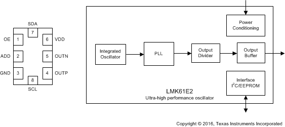
Pinout and Simplified Block Diagram
