SNVSAG9 March 2016 LM5022-Q1
PRODUCTION DATA.
- 1 Features
- 2 Applications
- 3 Description
- 4 Revision History
- 5 Pin Configuration and Functions
- 6 Specifications
- 7 Detailed Description
-
8 Application and Implementation
- 8.1 Application Information
- 8.2
Typical Application
- 8.2.1 Design Requirements
- 8.2.2
Detailed Design Procedure
- 8.2.2.1 Switching Frequency
- 8.2.2.2 MOSFET
- 8.2.2.3 Output Diode
- 8.2.2.4 Boost Inductor
- 8.2.2.5 Output Capacitor
- 8.2.2.6 VCC Decoupling Capacitor
- 8.2.2.7 Input Capacitor
- 8.2.2.8 Current Sense Filter
- 8.2.2.9 RSNS, RS2 and Current Limit
- 8.2.2.10 Control Loop Compensation
- 8.2.2.11 Efficiency Calculations
- 8.2.3 Application Curves
- 9 Power Supply Recommendations
- 10Layout
- 11Device and Documentation Support
- 12Mechanical, Packaging, and Orderable Information
Package Options
Mechanical Data (Package|Pins)
- DGS|10
Thermal pad, mechanical data (Package|Pins)
Orderable Information
1 Features
- AEC-Q100 Grade 1 Qualified with the following results:
- Device Temperature Grade 1: -40°C to 125°C Ambient Operating Temperature Range
- Device HBM ESD Classification Level 2
- Device CDM ESD Classification Level C5
- Internal 60-V Start-Up Regulator
- 1-A Peak MOSFET Gate Driver
- VIN Range: 6 V to 60 V (operate down to 3 V after startup)
- Duty Cycle Limit of 90%
- Programmable UVLO with Hysteresis
- Cycle-by-Cycle Current Limit
- Single Resistor Oscillator Frequency Set
- Adjustable Switching Frequency to 2.2MHz
- External Clock Synchronization
- Slope Compensation
- Adjustable Soft Start
- 10-Pin VSSOP Package
2 Applications
- Boost Converter
- SEPIC Converter
3 Description
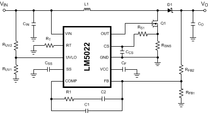
The LM5022-Q1 is a high voltage low-side N-channel MOSFET controller ideal for use in boost and SEPIC regulators. It contains all of the features needed to implement single-ended primary topologies. Output voltage regulation is based on current-mode control, which eases the design of loop compensation while providing inherent input voltage feed-forward. The LM5022-Q1 includes a start-up regulator that operates over a wide input range of 6 V to 60 V. The PWM controller is designed for high-speed capability including an oscillator frequency range up to 2.2 MHz and total propagation delays less than 100 ns. Additional features include an error amplifier, precision reference, line undervoltage lockout, cycle-by-cycle current limit, slope compensation, soft-start, external synchronization capability, and thermal shutdown. The LM5022-Q1 is available in the 10-pin VSSOP package.
Device Information(1)
| PART NUMBER | PACKAGE | BODY SIZE (NOM) |
|---|---|---|
| LM5022-Q1 | VSSOP (10) | 3.00 mm × 3.00 mm |
- For all available packages, see the orderable addendum at the end of the data sheet.
Typical Application
