SNVS569C May   2009  – October 2016 LM3550

PRODUCTION DATA.  

  1. Features
  2. Applications
  3. Description
  4. Revision History
  5. Pin Configuration and Functions
  6. Specifications
    1. 6.1 Absolute Maximum Ratings
    2. 6.2 ESD Ratings
    3. 6.3 Recommended Operating Conditions
    4. 6.4 Thermal Information
    5. 6.5 Electrical Characteristics
    6. 6.6 Timing Requirements
    7. 6.7 Typical Characteristics
  7. Detailed Description
    1. 7.1 Overview
    2. 7.2 Functional Block Diagram
    3. 7.3 Feature Description
      1. 7.3.1 STROBE Pin
      2. 7.3.2 End-of-Charge Pin (EOC)
      3. 7.3.3 ALD/TEMP Pin
      4. 7.3.4 IND Pin
      5. 7.3.5 BAL Pin
      6. 7.3.6 Super-Capacitor Charging Time
      7. 7.3.7 Super-Capacitor Voltage Profile
      8. 7.3.8 Peak Flash Current
      9. 7.3.9 Maximum Flash Duration
    4. 7.4 Device Functional Modes
      1. 7.4.1 State Machine Description
        1. 7.4.1.1 Basic Description
        2. 7.4.1.2 Shutdown State
        3. 7.4.1.3 Torch State
        4. 7.4.1.4 Charge State
          1. 7.4.1.4.1 Fixed-Voltage-Charge Mode
          2. 7.4.1.4.2 Optimal Charge Mode
        5. 7.4.1.5 Torch and Charge State
        6. 7.4.1.6 Flash State
        7. 7.4.1.7 EOC Functionality
        8. 7.4.1.8 State Diagram FGATE = 1
        9. 7.4.1.9 Optimal Charge Mode vs Fixed Voltage Mode
          1. 7.4.1.9.1 Optimal Charge Mode vs Fixed Voltage Mode
    5. 7.5 Programming
      1. 7.5.1 I2C-Compatible Interface
        1. 7.5.1.1 Data Validity
        2. 7.5.1.2 Start and Stop Conditions
        3. 7.5.1.3 Transferring Data
        4. 7.5.1.4 I2C-Compatible Child Address: 0x53
    6. 7.6 Register Maps
      1. 7.6.1 Internal Registers
        1. 7.6.1.1 General Purpose Register Description
        2. 7.6.1.2 Current Control Register Description
        3. 7.6.1.3 Options Control Register Description
        4. 7.6.1.4 ALD/TEMP Sense High/Low Registers
  8. Application and Implementation
    1. 8.1 Application Information
    2. 8.2 Typical Application
      1. 8.2.1 Design Requirements
      2. 8.2.2 Detailed Design Procedure
        1. 8.2.2.1 Component Selection
          1. 8.2.2.1.1 Super-Capacitor
          2. 8.2.2.1.2 Boost Capacitors
          3. 8.2.2.1.3 Current Source FET
          4. 8.2.2.1.4 ALD/TEMP Components
            1. 8.2.2.1.4.1 NTC Selection
            2. 8.2.2.1.4.2 Ambient Light Sensor
          5. 8.2.2.1.5 Thermal Protection
      3. 8.2.3 Application Curves
  9. Power Supply Recommendations
  10. 10Layout
    1. 10.1 Layout Guidelines
    2. 10.2 Layout Example
  11. 11Device and Documentation Support
    1. 11.1 Device Support
      1. 11.1.1 Third-Party Products Disclaimer
      2. 11.1.2 Device Nomenclature
    2. 11.2 Related Documentation
    3. 11.3 Receiving Notification of Documentation Updates
    4. 11.4 Community Resources
    5. 11.5 Trademarks
    6. 11.6 Electrostatic Discharge Caution
    7. 11.7 Glossary
  12. 12Mechanical, Packaging, and Orderable Information

Package Options

Mechanical Data (Package|Pins)
Thermal pad, mechanical data (Package|Pins)
Orderable Information

1 Features

  • Up to 5 A Flash Current
  • 4 Selectable Super-Capacitor Charge Voltage Levels (4.5 V, 5 V, 5.3 V, Optimized)
  • Adjustable Torch Current (60 mA to 200 mA)
  • Ambient Light or LED Thermal Sensing With Current Scaleback
  • Dedicated Indicator LED Current Source
  • No Inductor Required
  • Programmable Flash Pulse Duration, and Torch and Flash Currents via I2C-Compatible Interface
  • True Shutdown (LED Disconnect)
  • Flash Timeout Protection
  • Low Profile 20-Pin UQFN Package
    (3 mm × 2.5 mm × 0.8 mm)

2 Applications

  • Digital Still Camera
  • Voltage Rail Management
  • Fire Alarm Notification
  • Emergency Strobe Lighting
  • Intruder Alert Notification
  • Barcode Scanner
  • Handheld Data Terminal

3 Description

The LM3550 device is a low-noise, switched-capacitor DC-DC converter designed to operate as a current-limited and adjustable (up to 5.3 V) super-capacitor charger. The LM3550 features user-selectable termination voltages and provides one adjustable constant current output (up to 200 mA) and one NFET controller ideal for driving one or more high-current LEDs in a high-power flash mode or a low-power torch mode.

The LED current and flash pulse duration of the LM3550 can be programmed via an I2C-compatible interface. The STROBE pin allows the flash to be toggled via a flash-enable signal from a controller or camera module. The EOC pin sinks current when the output voltage reaches 95% of the final value.

The ALD/TEMP input pin allows either a light sensor to adjust the flash-current level based on the ambient light conditions, or it allows for overtemperature detection and protection of the LED during high-power operation or high ambient-temperature conditions.

Device Information(1)

PART NUMBER PACKAGE BODY SIZE (NOM)
LM3550 UQFN (16) 3.00 mm × 2.50 mm
  1. For all available packages, see the orderable addendum at the end of the data sheet.

Typical Application
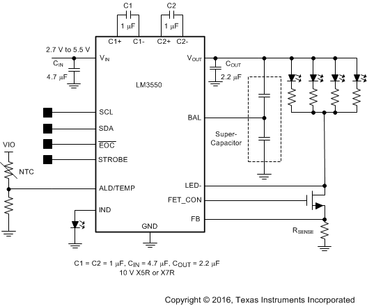
LM3550 30059401.gif