SNVS714F April 2011 – August 2015 LM25117 , LM25117-Q1
PRODUCTION DATA.
- 1 Features
- 2 Applications
- 3 Description
- 4 Revision History
- 5 Pin Configuration and Functions
- 6 Specifications
-
7 Detailed Description
- 7.1 Overview
- 7.2 Functional Block Diagram
- 7.3
Feature Description
- 7.3.1 High Voltage Startup Regulator and VCC Disable
- 7.3.2 UVLO
- 7.3.3 Oscillator And Sync Capability
- 7.3.4 Ramp Generator and Emulated Current Sense
- 7.3.5 Error Amplifier and PWM Comparator
- 7.3.6 Soft-Start
- 7.3.7 Cycle-By-Cycle Current Limit
- 7.3.8 Hiccup Mode Current Limiting
- 7.3.9 HO and LO Drivers
- 7.3.10 Current Monitor
- 7.3.11 Maximum Duty Cycle
- 7.3.12 Thermal Protection
- 7.4 Device Functional Modes
-
8 Application and Implementation
- 8.1 Application Information
- 8.2 Typical Applications
- 8.3
Detailed Design Procedure
- 8.3.1 Feedback Compensation
- 8.3.2 Sub-Harmonic Oscillation
- 8.3.3 Design Requirements
- 8.3.4 Timing Resistor RT
- 8.3.5 Output Inductor LO
- 8.3.6 Diode Emulation Function
- 8.3.7 Current Sense Resistor RS
- 8.3.8 Current Sense Filter RCS and CCS
- 8.3.9 Ramp Resistor RRAMP and Ramp Capacitor CRAMP
- 8.3.10 UVLO Divider RUV2, RUV1 and CFT
- 8.3.11 VCC Disable and External VCC Supply
- 8.3.12 Power Switches QH and QL
- 8.3.13 Snubber Components RSNB and CSNB
- 8.3.14 Bootstrap Capacitor CHB and Bootstrap Diode DHB
- 8.3.15 VCC Capacitor CVCC
- 8.3.16 Output Capacitor CO
- 8.3.17 Input Capacitor CIN
- 8.3.18 VIN Filter RVIN, CVIN
- 8.3.19 Soft-Start Capacitor CSS
- 8.3.20 Restart Capacitor CRES
- 8.3.21 Output Voltage Divider RFB2 and RFB1
- 8.3.22 Loop Compensation Components CCOMP, RCOMP and CHF
- 8.4 Application Curves
- 9 Power Supply Recommendations
- 10Layout
- 11Device and Documentation Support
- 12Mechanical, Packaging, and Orderable Information
Package Options
Mechanical Data (Package|Pins)
Thermal pad, mechanical data (Package|Pins)
Orderable Information
1 Features
- LM25117-Q1 is Qualified for Automotive Applications
- AEC-Q100 Qualified With the Following Results:
- Device Temperature Grade 1: -40°C to 125°C Ambient Operating Temperature Range
- Emulated Peak Current Mode Control
- Wide Operating Range from 4.5 V to 42 V
- Robust 3.3 A Peak Gate Drives
- Adaptive Dead-time Output Driver Control
- Free-run or Synchronizable Clock up to 750 kHz
- Optional Diode Emulation Mode
- Programmable Output from 0.8 V
- Precision 1.5% Voltage Reference
- Analog Current Monitor
- Programmable Current Limit
- Hiccup Mode Over Current Protection
- Programmable Soft-start and Tracking
- Programmable Line Undervoltage Lockout
- Programmable Switch-over to External Bias Supply
- Thermal Shutdown
2 Applications
- Automotive Infotainment
- Industrial DC-DC Motor Drivers
- Automotive USB Power
- Telecom Server
3 Description
The LM25117 is a synchronous buck controller intended for step-down regulator applications from a high voltage or widely varying input supply. The control method is based upon current mode control utilizing an emulated current ramp. Current mode control provides inherent line feed-forward, cycle-by-cycle current limiting and ease of loop compensation. The use of an emulated control ramp reduces noise sensitivity of the pulse-width modulation circuit, allowing reliable control of very small duty cycles necessary in high input voltage applications.
The operating frequency is programmable from 50 kHz to 750 kHz. The LM25117 drives external high-side and low-side NMOS power switches with adaptive dead-time control. A user-selectable diode emulation mode enables discontinuous mode operation for improved efficiency at light load conditions. A high voltage bias regulator that allows external bias supply further improves efficiency. The LM25117’s unique analog telemetry feature provides average output current information. Additional features include thermal shutdown, frequency synchronization, hiccup mode current limit and adjustable line undervoltage lockout.
Device Information(1)
| PART NUMBER | PACKAGE | BODY SIZE (NOM) |
|---|---|---|
| LM25117 |
HTSSOP (20) PWP | 6.50 mm x 4.40 mm |
| LM25117-Q1 | WQFN (24) RTW | 4.00 mm x 4.00 mm |
- For all available packages, see the orderable addendum at the end of the datasheet.
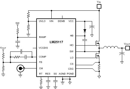
Typical Application
